A.2.1. CFI Flash Memory
A.2.1.1. CFI Flash Memory Map
Table 13. Byte Address Flash Memory Map
This table shows the default memory contents of the 512 Mb CFI flash device.
Address Range KB Size Block Description
0x0145.635C – 03FF.FFFF 44,711 Unused
0x00DA.0000 – 0145.635B 6,872 User hardware 2
0x006E.0000 – 00D9.635B 6,872 User hardware 1
0x0002.0000 – 006D.635B 6,872 Factory hardware
0x0001.8000 – 0001.8080 32 PFL option bits
Caution: Altera recommends that you do not overwrite the factory hardware images unless you
are an expert with Altera tools. If you unintentionally overwrite the factory hardware
or factory software image, refer to the Restoring the CFI Flash Device to the Factory
Defaults section.
Related Information
Restoring CFI Flash Device to the Factory Defaults on page 22
A.2.1.2. Programming CFI Flash Using the Quartus Prime Programmer
You can use the JTAG interface in Altera CPLDs to indirectly program the flash memory
device. The Altera CPLD JTAG block interfaces directly with the logic array in a special
JTAG mode.
This mode brings the JTAG chain through the logic array instead of the Altera CPLD
boundary-scan cells (BSC). The Parallel Flash Loader Intel FPGA IP provides JTAG
interface logic to do the following:
• Convert the JTAG stream provided by the Quartus Prime software.
• Program the CFI flash memory devices connected to the CPLD I/O pins.
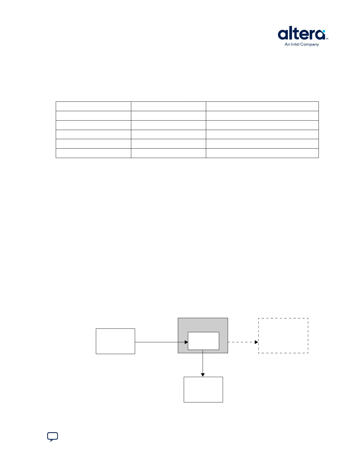
Figure 20. Programming the CFI Flash Memory With the JTAG Interface
Shows an Altera CPLD configured as a bridge to program the CFI flash memory device through the JTAG
interface.
Altera®
FPGA
MAX® II CPLD
Common
Flash
Interface
CFI Flash
Memory
Quartus® Prime
Software
via JTAG
Altera FPGA Not Used
for Flash Programming
Parallel Flash
Loader (PFL)
Configuration Data
A. Development Kit Components
830285 | 2024.10.07
Send Feedback
Cyclone
®
V SoC Development Kit User Guide
47