3-2 Intel
®
Pentium
®
III Processor with 512KB L2 Cache Dual Processor Platform Design Guide
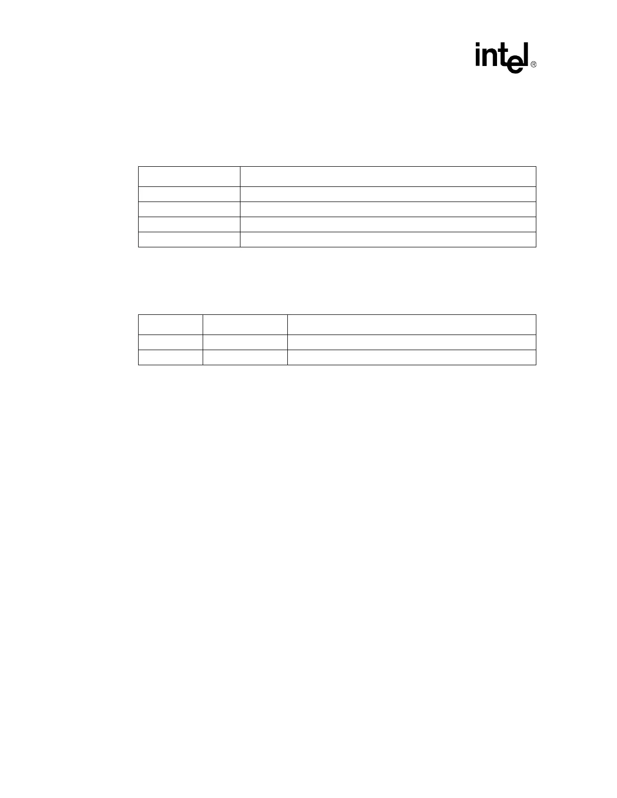
Recommended values for system timings are contained in Table 3- 3. Skew and jitter values for the clock
generator device come from the clock driver datasheet. The PCB skew specification is based on the
results of extensive simulations at Intel. The T
adj
value is based on Intel’s experience with systems that
use previous generations of processors.
The flight time requirements for CPU to CPU transfers that result from using the component timing
specifications and recommended system timings are summarized in Table 3-4. All component values
should be verified against the latest specifications before proceeding with analysis.
3.2 General Topology and Layout Guidelines
Intel is recommending that all Intel
®
Pentium
®
III Processor with 512KB L2 Cache dual-processing
platforms use a system bus T-topology. Figure 3-1 shows a high level diagram of this topology. The pull-
up resistors shown inside the processor packages are the processor’s on-die AGTL termination. Since
the processor has on-die termination, a dual processor capable system must either have two processors
installed, or one processor and one terminator.
Table 3-3. System Bus Timing Parameters
Timing Term Value
T
skew
[ns] 0.250
T
jit
[ns] 0.2
T
adj
[ns] 0.5
T
cycle
[ns] 7.5
Table 3-4. Sample CPU to CPU flight time calculations
Driver Receiver Calculation
CPU CPU T
flight,min
>= 1.0 - 0.4 + 0.25 = 0.85 ns
CPU CPU T
flight,max
<= 7.5 - 3.25 - 0.95 - 0.25 - 0.2 - 0.5 = 2.35 ns