4-4 Intel
®
Pentium
®
III Processor with 512KB L2 Cache Dual Processor Platform Design Guide
The following guidelines should also be followed for single-ended clock implementations:
• BCLK must be routed through trace impedance of 60 ohm +/- 10%.
• Use 5 mil wide traces.
• Place all serial termination resistors within 0.50 inches to clock driver pins.
• Place all other signals at least 20 mils from the clock traces.
• All the termination resistors are rated at 1% accuracy.
• The two processor clock traces should be matched to within 0.250 inches.
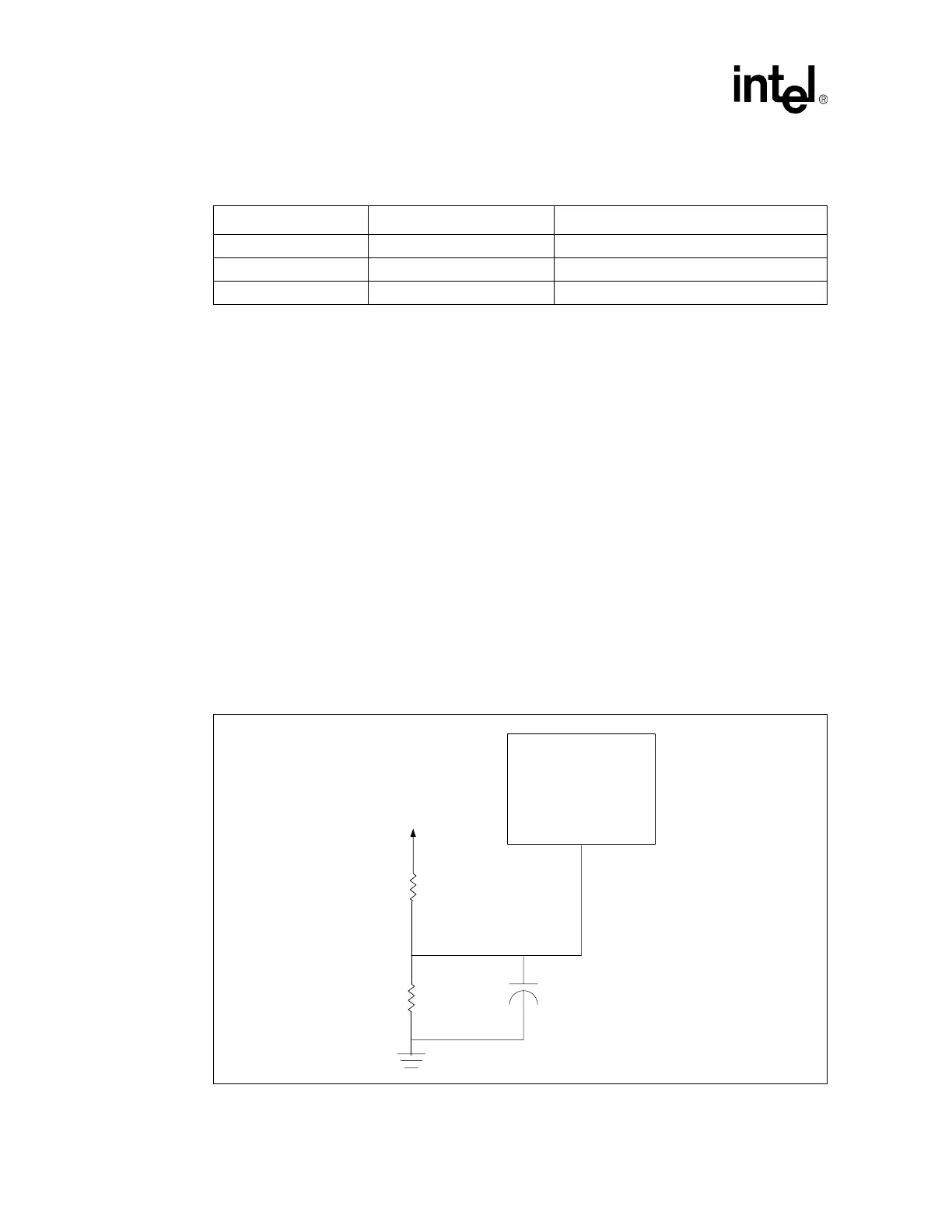
4.2.1 CLKREF Filter Implementation
When using single-ended clocking mode, the BCLK#/CLKREF signal on the processor serves as a
reference voltage to the clock input. To provide a steady reference voltage, a filter circuit must be
implemented and attached to this pin. Figure 4-4 shows the recommended CLKREF filter
implementation. The CLKREF filter should be placed as close as possible (less that 1.0 inch) to the
processor’sCLKREFpin.
Table 4-2. Component Values for SE Clocking Topology - Chipset
Reference Value Notes
L0 0.25 to 0.5 inches All L0s should be matched
L1 5 inches to 12 inches Effects processor lengths.
Rs 22 to 33 Ω 1% Tolerance
Figure 4-4. CLKREF Filter Implementation
Vcc2.5
PGA370
CLKREF
R1
Y33
R2
C1