Intel
®
Pentium
®
III Processor with 512KB L2 Cache Dual Processor Platform Design Guide 8-3
8.5 TAP/ITP Checklist for 370-Pin Socket Processors
There are several mechanical, electrical, and functional constraints on the debug port which must be
followed, please see the Intel
®
Pentium
®
III Processor with 512KB L2 Cache Datasheet,alongwith
Chapter 3 of this document for details.
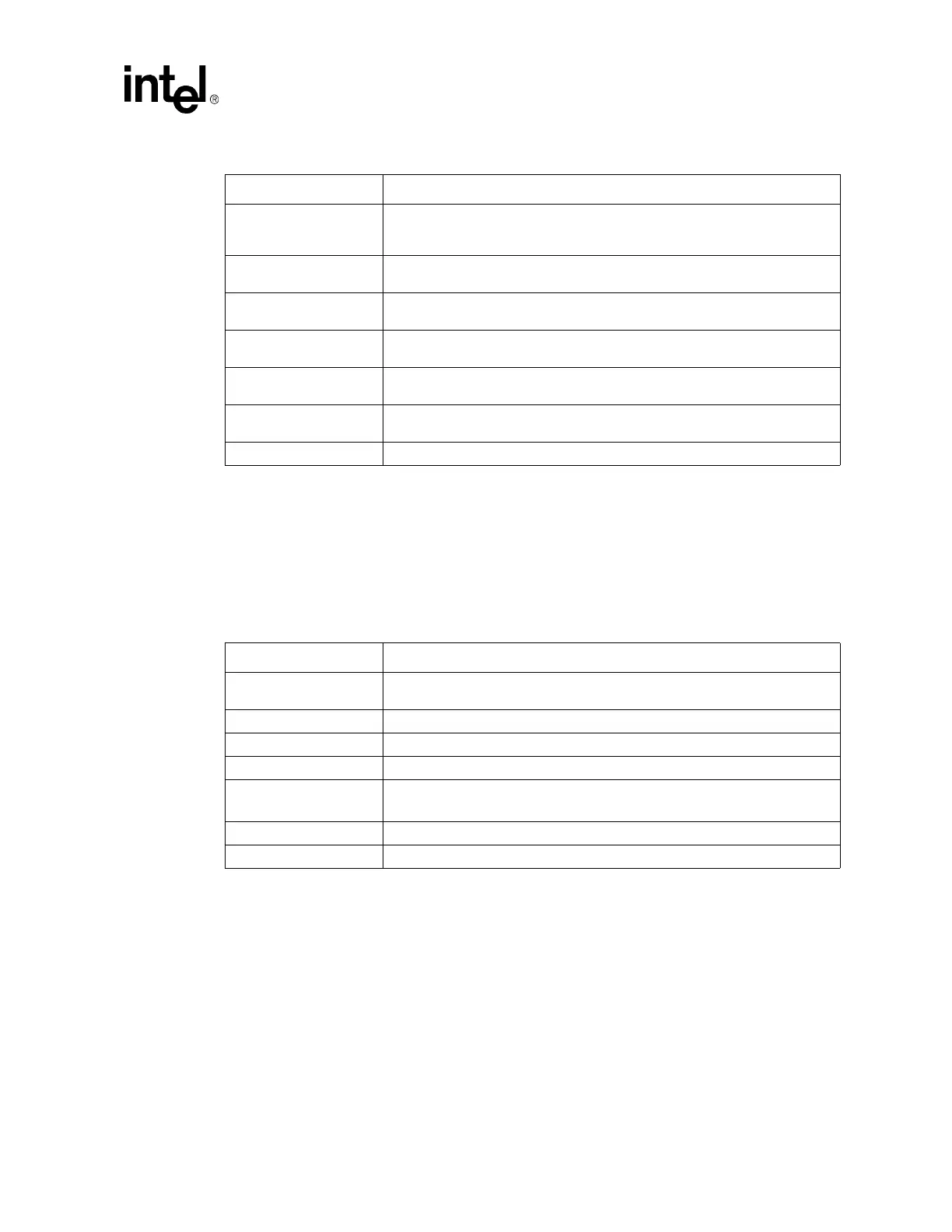
LINT1/NMI
Connect to interrupt control logic and second CPU and pull up through ~330 Ω to
VccCMOS. For boards supporting preproduction processors, this pin must be
connected to frequency selection circuitry.
PICD[1:0]
Connect to second CPU and pull up through ~150 Ω to VccCMOS. May also
need to be connect to interrupt control logic.
PWRGOOD
Connect to second CPUs and pull up through 150-330 Ω to 1.8 V. output from the
PWRGOOD logic.
SLP#
Connect to second CPU and pull up through ~330 Ω to Vcc
CMOS1.5
. May also
need to be connected to chipset or compatibility logic.
SMI#
Connect to second CPU and pull up through ~330 Ω to Vcc
CMOS1.5
. May also
need to be connected to chipset or compatibility logic.
STPCLK#
Connect to second CPU and pull up through ~330 Ω to Vcc
CMOS1.5
. May also
need to be connected to chipset or compatibility logic.
THERMTRIP# See Chapter 6 for more information.
Table 8-3. TAP/ITP Signals
CPU Pin Pin Connection
PRDY#
Pull-up resistor that matches GTL characteristic impedance to VTT, 240 Ω series
resistor to ITP.
PREQ# 200-300 Ω pull-up to VccCMOS and connect to ITP.
TCK 39 Ω pull-down to Gnd, and connect to ITP.
TDO 150 Ω pull-up to VccCMOS and connect to ITP.
TDI
200-300 Ω pull-up to VccCMOS and connect to ITP.
Connect TDI from CPU0 to TDO on CPU1.
TMS 39 Ω pull-up to VccCMOS and connect to ITP.
TRST# 500-680 Ω pull-down to Gnd and connect to ITP.
Table 8-2. CMOS Signals (Sheet 2 of 2)
CPU Pin Pin Connection