3-10 Intel
®
Pentium
®
III Processor with 512KB L2 Cache Dual Processor Platform Design Guide
resources and may be shared with local JTAG tools. Input and output signals are available. The
execution signals are a combination of CMOS and AGTL level signals. They are both inputs and outputs
to the ITP.
The ITP TCK and TMS signals must be routed with a maximum trace resistance of 2.0 ohm to reduce the
amount of DC shifting on these signals. This is due to the small termination values that are
recommended for these signals.
3.10.1.1.1 System Signal Layout Guidelines
Table 3- 10 provides the system signal layout guidelines. See Table 3-13 for termination values.
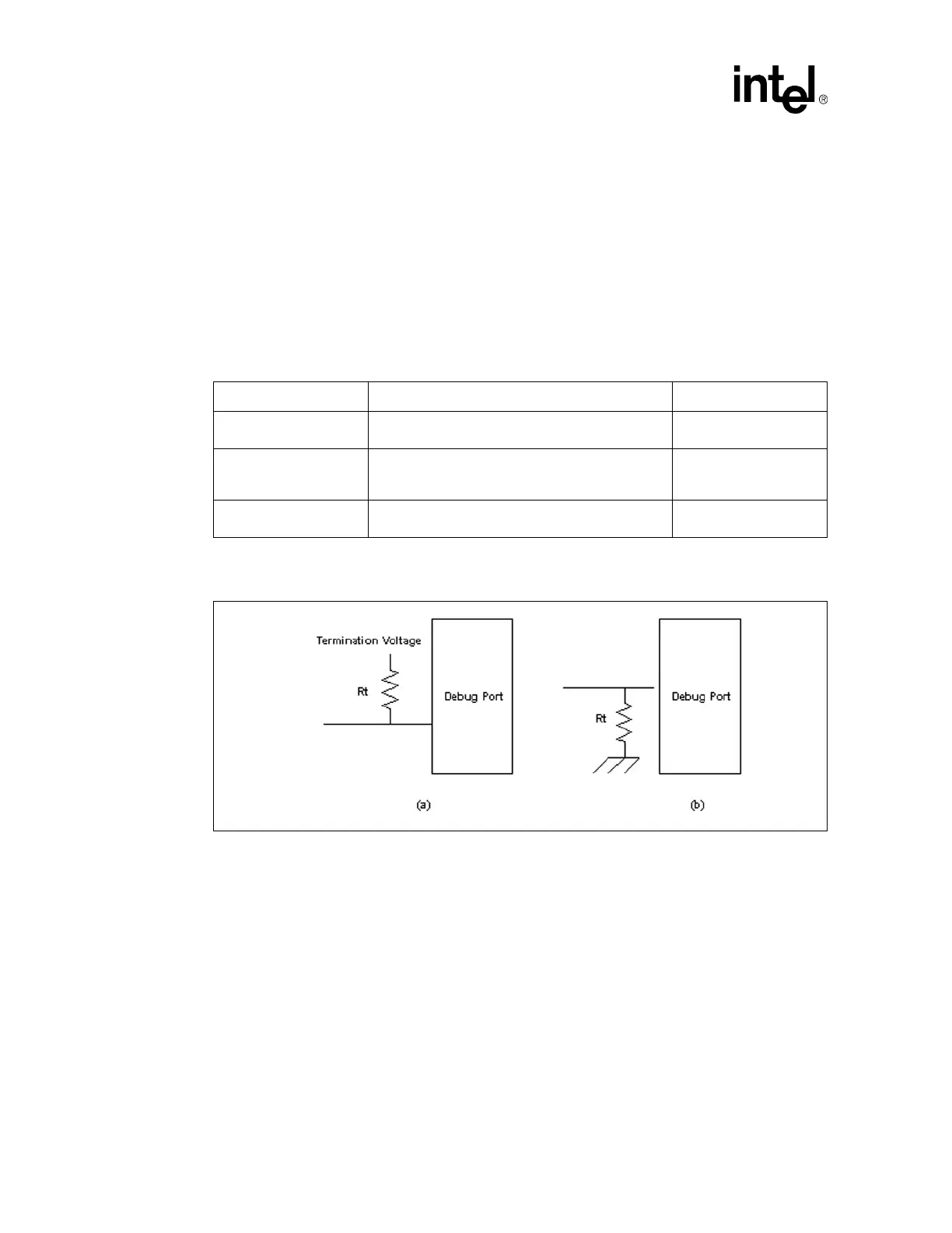
Table 3-10. System Signal Layout Guidelines
Signal Routing Notes Sample Layout
POWERON
Route with normal trace 2 to 6 inches to the debug
port connector
Figure 3-4a
BCLK, BCLK#
Refer to BCLK system requirements documentation
for proper termination values and routing
requirements
N/A
DBRESET#, BSEN#,
DBINST#
Figure 3-4a
Figure 3-4. Simple Terminations