Intel
®
Pentium
®
III Processor with 512KB L2 Cache Dual Processor Platform Design Guide 3-13
3.10.1.2 Signal Termination Requirements
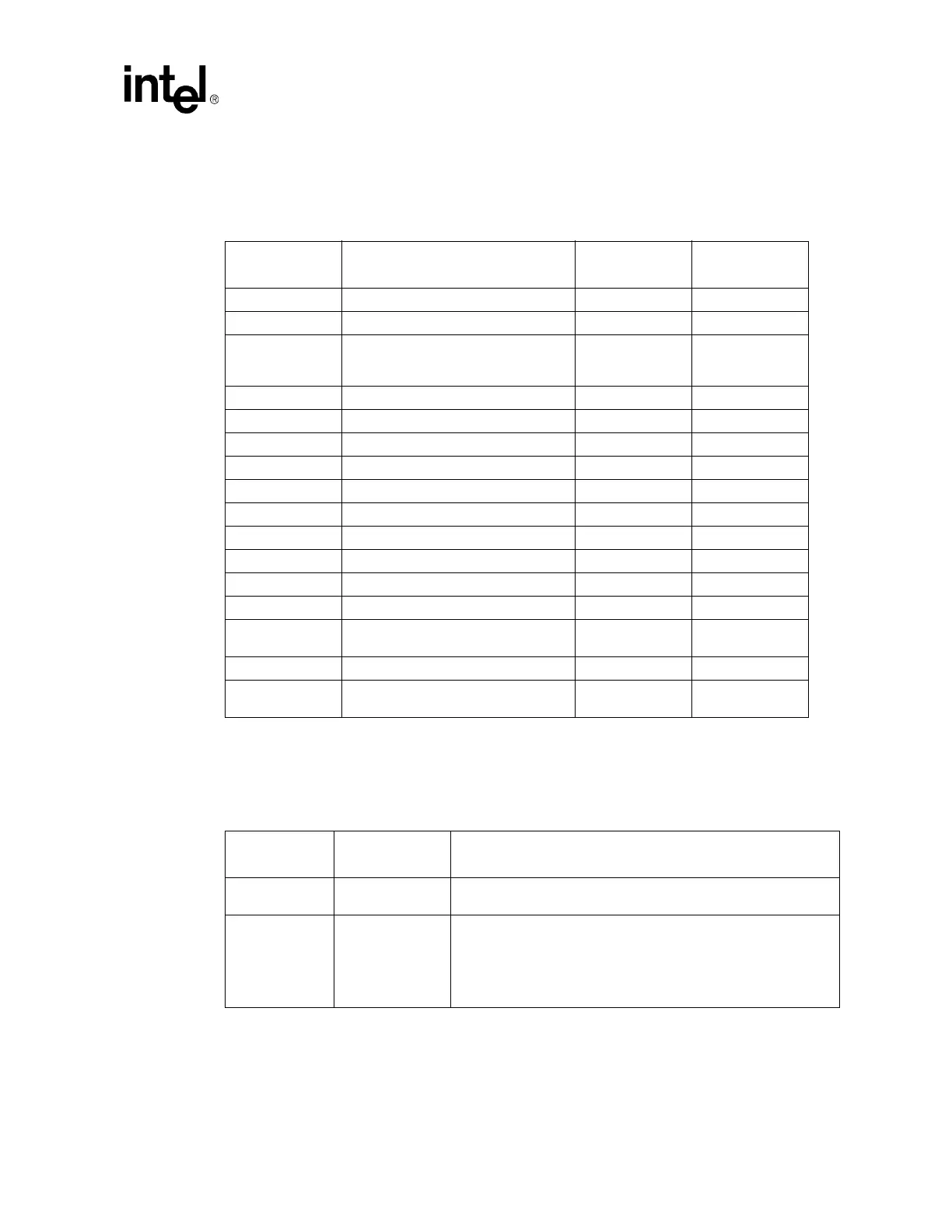
Table 3-13 lists signal termination requirements for the debug port signals.
3.10.1.3 Routing Guidelines
Table 3-13. Debug Port Termination Requirement
Signal Signal Termination Value (Rt)
Termination
Value (Rs)
Termination
Voltage
System Signal
POWERON 1.5 KΩ N/A V
TT
BCLK, BCLK#
Refer to BCLK system requirements
documentation for proper termination
values and routing requirements
BSEN# 240 Ω N/A V
CC
DBRESET# 240 Ω N/A V
CC
DBINST# 10 KΩ N/A V
CC
JTAG Signals
TCK 39 Ω GND
TDI 200 - 300 Ω N/A VCC
CMOS1.5
TDO 150 Ω N/A VCC
CMOS1.5
TMS 39 Ω N/A VCC
CMOS1.5
TRST# 500 - 680 Ω N/A GND
Execution signals
RESET#
Match to AGTL characteristic
impedance
240 Ω V
TT
PREQx# 200 - 300 Ω N/A Vcc
CMOS1.5
PRDYx#
Match to AGTL characteristic
impedance
240 Ω V
TT
Table 3-14. Routing Guidelines
Parameter
Reference
Figure
Description
TCK Figure 3-5
1" max from debug port to RT AND 12" max from debug port to
processor VERY SENSITIVE TO NOISE -- please route accordingly
TMS, TDO, TDI,
POWERON,
DBRESET#,
BSEN#,
DBINST#,
PREQx#
Figure 3-4
a
1" max from debug port to RT AND 12" max from debug port to
processor