4-6 Intel
®
Pentium
®
III Processor with 512KB L2 Cache Dual Processor Platform Design Guide
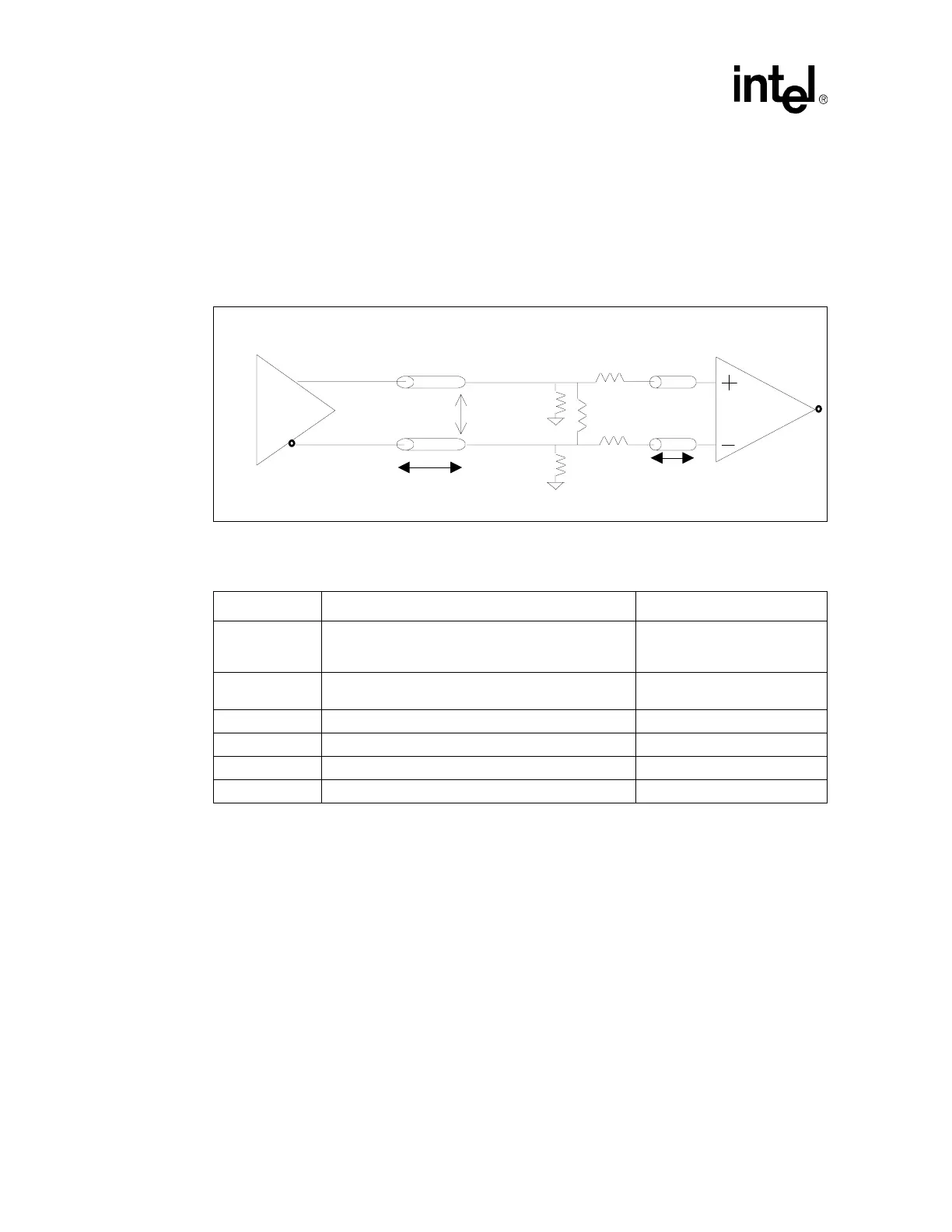
4.3.1 Differential Clocking Topology
Figure 4-6 shows the topology that should be used for the processor and chipset traces. Please note that
L0 and L1 refer to trace lengths between the illustrated components. Table 4- 4 contains the
recommended lengths and component values for this topology.
The following guidelines should also be followed for differential clock implementations:
• Match BCLK and BCLK# in length, width and impedance.
• BCLK and BCLK# should be coupled to achieve odd mode impedance of 50 ohm.
• Use 5 mil traces, routed differentially.
• Place all termination resistors within 0.40 inches of BCLK/BCLK# pins at the receiver.
• Other should be spaced at least 20 mils away from clock lines.
• All the termination resistors are rated as 1% accuracy.
• Minimize stubs to passive components.
• Clock to chipset is 1 inch longer than the clock to CPU (to compensate for CPU package load).
Figure 4-6. Differential Clocking Topology
Table 4-4. Component Values for Differential Clocking
Reference Value Notes
L0 (Processor) 5 to 9 inches
Match each processor
differential pair to within 0.250
inches
L0 (Chipset) Processor L0 + 1 inch +/- 0.125 inches
Match to the processor L0 and
add 1 inch for package loading
L1 0.0 to 0.4 inches Should be as short as possible
Rd 63.4Ω 1% Tolerance
Rs 33.2Ω 1% Tolerance
Rc 475Ω 1% Tolerance
BCLK
BCLK#
Clock Driver
Processor/Chipset
Rd
Rs
Rd
Zodd_mode = 50 ohm
Rs
Rc
L1
L0