Thin Mini-ITX Internal Electrical Interfaces
Thin Mini-ITX Based PC System Design Guide 33
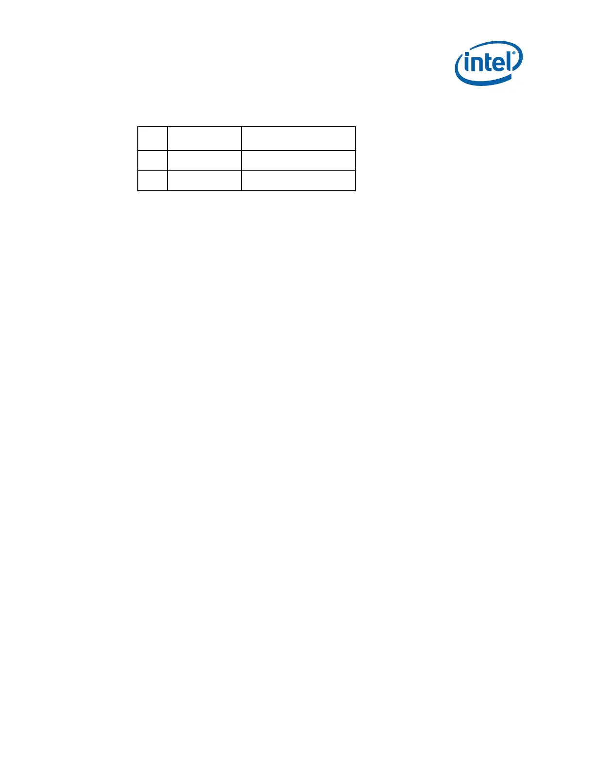
Table 2-15. Monitor Switch Header Pin-Out
For boards where the requirement is to simply turn the display off/on, a suggested
implementation is as follows:
MON_SW# input signal connects to PCH GPIO3 (pulled-up to +VCC3)
when the monitor switch button is pressed, PCH receives edge-trigger from
MON_SW# input. The system BIOS toggles the state of BKLT_OFF# upon this
event.
BKLT_OFF# output signal is driven out of PCH GPIO6 (pulled-up to +VCC3). This
signal wired to gate the BKLT_EN signal from enabling/disabling the
inverter/driver board.
Therefore, when the monitor switch button is momentarily pressed, MON_SW# sends
a signal to the BIOS which causes the BKLT_OFF# signal to toggle states (default is
BKLT_OFF# inactive, for backlight on). BKLT_OFF# output consequently allows the
panel’s backlight unit to be switched off/on.