Table of Contents
P/N 960-000180R_Rev. 1 {EDP #233427} © 2016, JAPAN CASH MACHINE CO., LTD.
Page
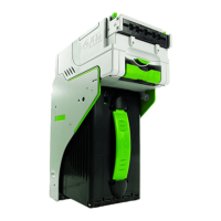
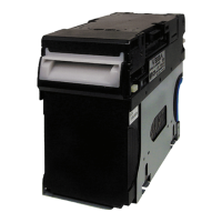
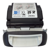
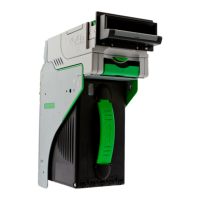
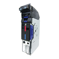
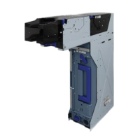
DBV® Series DBV-400 Banknote Validator
TTL Connector Pin Assignments................................................................................... 2-5
ID-002 Pulse Connector Pin Assignments .................................................................... 2-6
ID-044 Pulse Connector Pin Assignments .................................................................... 2-7
ID-044 Serial Connector Pin Assignments .................................................................... 2-8
USB Interface Connector Pin Assignments................................................................... 2-9
USB Maintenance Interface Connector Pin Assignment............................................... 2-9
Preventive Maintenance ........................................................................................... 2-10
Retrieving Banknotes .................................................................................................. 2-10
Clearing a Banknote Jam ............................................................................................ 2-10
Cleaning Procedure......................................................................................................2-11
Sensor and Roller Cleaning Procedure ...................................................................................2-11
Sensor and Roller Locations................................................................................................... 2-12
Standard Interface Circuit Schematics.................................................................... 2-13
Standard Interface Circuit Schematics (Continued 1).................................................. 2-14
Standard Interface Circuit Schematics (Continued 2).................................................. 2-15
Standard Interface Circuit Schematics (Continued 3).................................................. 2-16
Standard Interface Circuit Schematics (Continued 4).................................................. 2-17
Standard Interface Circuit Schematics (Continued 5).................................................. 2-18
Standard Interface Circuit Schematics (Continued 6).................................................. 2-19
Operational Flowchart .............................................................................................. 2-21
Operational Flowchart (Continued 1) .......................................................................... 2-22
3 COMMUNICATIONS ............................................................................................3-1
Americas................................................................................................................................... 3-1
JCM American........................................................................................................................ 3-1
Europe, Middle East, Africa & Russia ....................................................................................... 3-1
JCM Europe GmbH................................................................................................................ 3-1
UK & Ireland ............................................................................................................................. 3-1
JCM Europe (UK Office)......................................................................................................... 3-1
Asia and Oceania ..................................................................................................................... 3-1
JCM Gold (HK) Ltd. ................................................................................................................ 3-1
Japan Cash Machine Co., Ltd. (HQ) ...................................................................................... 3-1
4 DISASSEMBLY/REASSEMBLY ..........................................................................4-1
Tool Requirements ...................................................................................................... 4-1
CPU Circuit Board Removal ....................................................................................... 4-1
Side Sensor Removal.................................................................................................. 4-2
Motor Harness Assy. Removal ................................................................................... 4-2
Inside Validation Sensor Board Removal ................................................................. 4-2
Outside Validation Sensor Board Removal............................................................... 4-3
Box Base Assy. Removal............................................................................................ 4-4
5 WIRING DIAGRAMS ............................................................................................5-1
System Wiring Diagram .............................................................................................. 5-1
6 CALIBRATION AND TESTING ............................................................................6-1
Tool Requirement ........................................................................................................ 6-1
Workbench Tool Requirements With Reference Paper and a PC................................. 6-1
Workbench Tool Requirements Without a PC ............................................................... 6-1