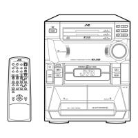
MX-J170V
1-38
SymbolPin No. Function
HFREF1 comparator common mode input
HFIN2 comparator signal input
ISLICE3 current feedback output from data slicer
V
SSA1
4
(1)
analog ground 1
V
DDA1
5
(1)
analog supply voltage 1
I
ref
6 reference current output
V
RIN
7 reference voltage for servo ADCs
D18 unipolar current input 1 (central diode signal input)
D29 unipolar current input 2 (central diode signal input)
D310 unipolar current input 3 (central diode signal input)
D411 unipolar current input 4 (central diode signal input)
R112 unipolar current input 1 (satellite diode signal input)
R213 unipolar current input 2 (satellite diode signal input)
V
SSA2
14
(1)
analog ground 2
CROUT15 crystal/resonator output
CRIN16 crystal/resonator input
V
DDA2
17
(1)
analog supply voltage 2
LN18 DAC left channel differential negative output
LP19 DAC left channel differential positive output
V
neg
20 DAC negative reference input
V
pos
21 DAC positive reference input
RN22 DAC right channel differential negative output
RP23 DAC right channel differential positive output
SELPLL24 selects whether internal clock multiplier PLL is used
TEST125 test control input 1 (this pin should be tied LOW)
CL1626 16.9344 MHz system clock output
DATA27 serial d4(1) data output (3-state)
WCLK28 word clock output (3-state)
SCLK29 serial bit clock output (3-state)
EF30 C2 error ßag output (3-state)
TEST231 test control input 2 (this pin should be tied LOW)
KILL32 kill output (programmable; open-drain)
V
SSD1
33
(1)
digital ground 1
V2/V334 versatile I/O: versatile input 2 or versatile output 3 (open-drain)
WCLI35 word clock input (for data loopback to DAC)
SDI36 serial data input (for data loopback to DAC)
SCLI37 serial bit clock input (for data loopback to DAC)
RESET38 power-on reset input (active LOW)
SDA39 microcontroller interface data I/O line (I
2
C-bus; open-drain output)
SCL40 microcontroller interface clock line input (I
2
C-bus)
2. Pin function