Do you have a question about the JVC RX-807VTN and is the answer not in the manual?
Installation, power handling, and malfunction precautions for the stereo system.
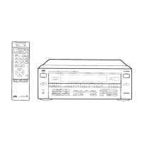
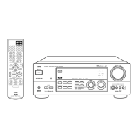
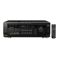
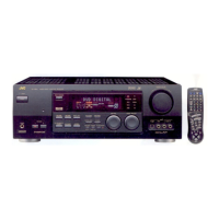
Details on using buttons on the remote's external panel for basic functions.
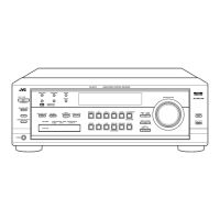
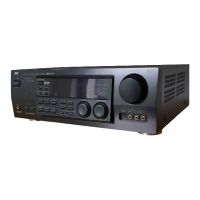
Information on accessing advanced programming and control functions on the internal panel.
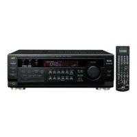
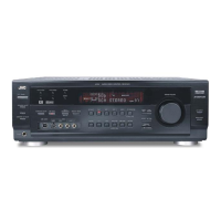
Pre-operation checks including component connection and remote sensor usage.
Explains how to use cursor keys for navigation and control across different sources.
Instructions on setting the sleep timer to automatically turn off the receiver.
Procedures for tuning AM and FM radio stations using the receiver.
Guide on storing favorite AM/FM stations into memory for quick access.
How to automatically scan and preset radio stations based on signal strength.
How to select and use pre-programmed or custom sound equalization patterns.
Steps to adjust frequency bands and save custom equalization settings.
Instructions for recording SEA-corrected audio onto a tape deck.
How to name SEA preset patterns and tuner channels using the front panel.
Procedures for copying audio between different tape decks or sources.
Recommended speaker placement for optimal surround sound effect.
Explanation of the Dolby Pro Logic decoder and its sound enhancement capabilities.
Adjusting rear and center speaker levels for maximum surround effect.
Setting the delay time for rear speakers relative to front speakers.
How to store volume, surround, and SEA settings for each source.
Controlling JVC components via the receiver's remote sensor.
How the receiver automatically selects input sources for connected components.
Permitting tape decks to start recording automatically with CD players or turntables.
Automatically powering on and playing video tapes by loading them into the VCR.
Coordinating power states between the receiver, TV, and VCR.
Using the remote to control CD playback functions like play, stop, and track skipping.
Controlling VCR playback, recording, and tape winding functions.
Operating the tape deck functions such as play, rewind, and fast-forward.
Step-by-step instructions for removing the unit's top cover.
Guide on how to detach the front panel from the receiver.
Procedures for removing the FL display circuit board.
Steps to remove the bottom plate from the receiver.
Instructions for removing power transistors from the main and center amplifiers.
Guide on how to remove the rear amplifier module.
Setting the idling current for the power amplifier stages.
Verifying surround effect waveforms by connecting an oscilloscope.
Procedures for aligning the FM oscillator, antenna coil, and detector circuits.
Steps for aligning the MW oscillator, antenna coil, and trimmer circuits.
Procedures for aligning the LW oscillator, antenna coil, and trimmer circuits.
Pinout diagram and terminal functions for major integrated circuits.
Mapping of key inputs to the internal matrix for IC461.
Pinout diagram and layout for the LC6514B-4131 IC.
Key matrix mapping for the LC6514B-4131 IC.
Detailed pin function descriptions for the LC6514B-4131 IC.
Block diagram for the XR1091DCP (IC432) display filter IC.
Block diagram for the TC74HC154P (IC462) decoder IC.
Main functions of the LC7218 (IC102) PLL synthesizer IC.
Pinout diagram for the LC7218 (IC102) PLL synthesizer IC.
Block diagram illustrating the internal structure of the LC7218 IC.
Main functions of the LA1266A (IC104) FM/AM IF AMP IC.
Block diagram of the LA1266A (IC104) FM/AM IF AMP.
Main functions of the LA3401 (IC105) FM MPX Detector IC.
Terminal layout for the LA3401 (IC105) FM MPX Detector IC.
Block diagram of the LA3401 (IC105) FM MPX Detector IC.
Explanation of the M50198P (IC651) Digital Delay IC's operation.
Block diagram of the M50198P (IC651) Digital Delay IC.
Terminal layout, block diagram, and function table for the A/D Converter IC.
Terminal layout and function table for the Shift Register IC.
Terminal layout, block diagram, and pin functions for the SEA Control IC.
Terminal layout for the Inverter IC.
Terminal layout and function table for the Video Selector IC.
Block diagram for the Dolby Pro Logic IC.
Terminal layout and pin functions for the FL Driver IC.
Terminal layout and block diagram for the Electro-volum IC.
Block diagram for the Power Amplifier IC.
Terminal layout and block diagram for the Protector IC.
Terminal layout and block diagram for the Super-A IC.
Pinout and layout of the FL display's terminal connections.
Mapping of pins to grid and anode segments for the FL display.
Assignment of signals to grid-anode pins for section A of the FL display.
Assignment of signals to grid-anode pins for section B of the FL display.
Assignment of signals to grid-anode pins for section C of the FL display.
Overall signal path diagram showing audio and control signal flow.
Component placement and routing diagram for the ENC-093 circuit board.
Component layout diagram for the ENH-204 Power Amplifier and Power Supply PCB.
Component placement diagram for the ENB-155 System Control & FL PCB.
Component layout diagram for the ENA-095 Tuner PC Board.
An overall visual breakdown of the unit's components and their part numbers.
Lists of parts specifically for the main circuit boards (ENH, ENC, ENA, ENB).
List of included accessories such as manuals, warranty cards, and cables.
| Channels | 5.1 |
|---|---|
| Speaker load impedance | 8 ohms |
| Video Connections | composite, S-Video |
| Weight | 12.5 kg |
| Power Output | 100 watts per channel |
| Tuning range | FM |
| Frequency Response | 10 Hz - 100 kHz |
| Input Sensitivity | 200 mV |
| Inputs | 1 x phono |
| Outputs | 1 x headphone |