11
ECP5 and ECP5-5G High-Speed I/O Interface
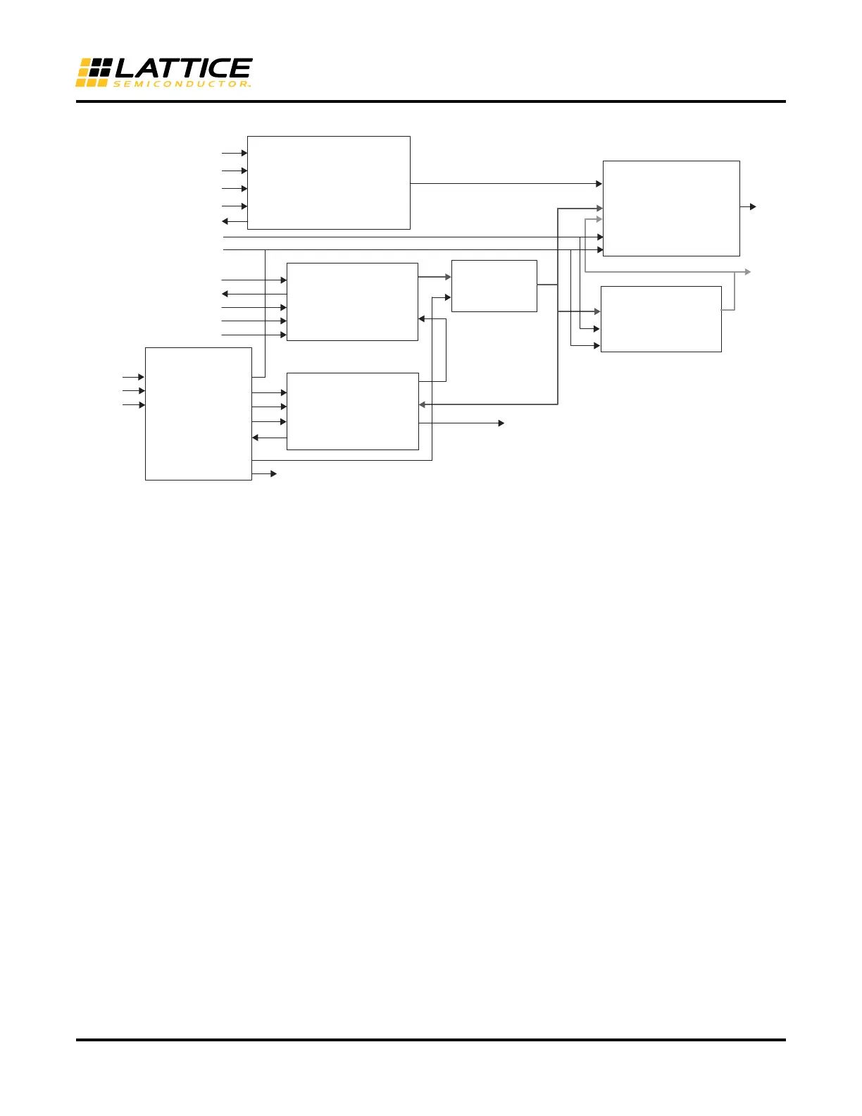
Figure 11. GDDRX2_RX.ECLK.Aligned Interface (Dynamic Data/Clock Delay)
Interface Requirements
• The clock input must use a dedicated PCLK input so that it can be routed directly to the DLLDEL module
• ECLK must use the Edge clock tree and the SCLK out of the CLKDIVD must use the Primary clock tree, software
will error out if these dedicated clock routes are not used
• “USE PRIMARY” preference may be assigned to the SCLK net
• The user must set the timing preferences as per section “Timing Analysis Requirement”
GDDRX2_RX.MIPI
Generic Receive DDR for MIPI interfaces using the X2 gearing with ECLK. Clock is coming in centered to the Data.
This interface must be used for speeds above 200 MHz.
This DDR interface uses the following modules:
• IMIPI element use to receive the MIPI data and clock
• The HSSEL of the IMIPI is used to switch between the High speed and Low Speed modes
• The HSSEL of IMIPI should be driven by a soft IP
• When in high speed mode
– The OHSOLS1 of the element is active
– The OHSOLS1 of the data IMIPI element is connected to the Data input GDDRX2_RX.ECLK.Centered
Interface
– The OHSOLS1 of the clock IMIPI is connected to the ECLK input GDDRX2_RX.ECLK.Centered Interface
– This is then treated similar to the GDDRX2_RX.ECLK.Centered Interface
• When in low speed mode:
– Both the outputs of IMIPI are active since it is not a 2-bit interface
– The OHSLS1 is the bit 1 and OLS0 is the bit 0 of the interface.
– Each of the data input and clock input is connected through a 20ns filter soft IP to the core
Data_LoadN
Data_Move
Data_Direction
A
DELAYF
LOADN
MOVE
DIRECTION
CFLAG
Datain
Clkin
DDR_reset
DLLDELD
Z
A
DDRDEL
LOADN
MOVE
DIRECTION
CFLAG
CLK
RST
UDDCNTLN
FREEZE
DDRDEL
LOCK
DDRDLLA
DCNTL[7:0]
Dcntl[7:0]
Clock_LoadN
Clock_Move
Clock_Direction
Clock_CFlag
Data_CFlag
Z
ECLKI
STOP
ECLKO
SCLK
D
RST
ALIGNWD
ECLK
Edge
Primary
Sclk
CLKDIVF
CLKI
RST
ALIGNWD
CDIVX
AlignWD
Q[3:0]
Q[3:0]
IDDRX2F
ECLKSYNCB
(optional)
STOP
DLL_LOCK
FREEZE
UDDCNTLN
DLL_RESET
DDR_RESET
SYNC_CLK
RST
UPDATE
Sync_clk
Sync_rst
Update
READY
RX_SYNC
Ready
DEL_MODE=
ECLK_CENTERED
 Loading...


