14
ECP5 and ECP5-5G High-Speed I/O Interface
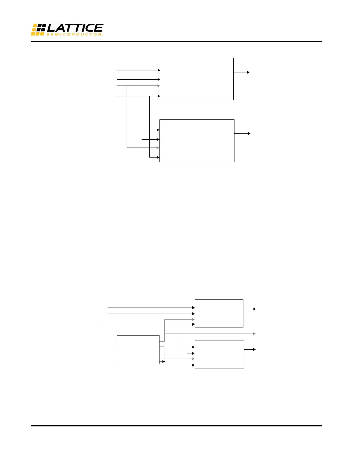
Figure 14. GDDRX1_TX.SCLK.Aligned Interface
Interface Requirements
• The clock to the output DDR modules must be routed on the primary clock tree
GDDRX1_TX.SCLK.Centered
Generic Transmit DDR using X1 gearing with SCLK. Clock output is centered to the Data output.
This DDR interface uses the following modules:
• ODDRX1F element is used to generate the data output
• The EHXPLLL element is used to generate the clocks for the data and clock ODDRX1F modules. The clock used
to generate the clock output is delayed 90 to center to data at the output.
• Both these clocks are routed on primary clock tree
• Optionally the user can choose to use the DELAYG or DELAYF element to delay the output data
• The output data can be optionally tristated using either a Tristate input going through an I/O register.
Figure 15. GDDRX1_TX.SCLK.Centered Interface
Interface Requirements
• The clock to the output DDR modules must be routed on the primary clock tree
D0
D1
SCLK
RST
Q
ODDRX1F
Data[1:0]
D0
D1
SCLK
RST
Q
ODDRX1F
1'b1
1'b0
Refclk
Reset
Dout
Clkout
Primary
Reset
D0
D1
SCLK
RST
Q
ODDRX1F
Data [1:0]
D0
D1
SCLK
RST
Q
ODDRX1F1
1'b 1
1'b 0
Refclk
Dout
Clkout
Primary
Primary
EHXPLLK
CLKOP
CLKI
RST
CLKOS
LOCK
Sclk
 Loading...


