66
ECP5 and ECP5-5G High-Speed I/O Interface
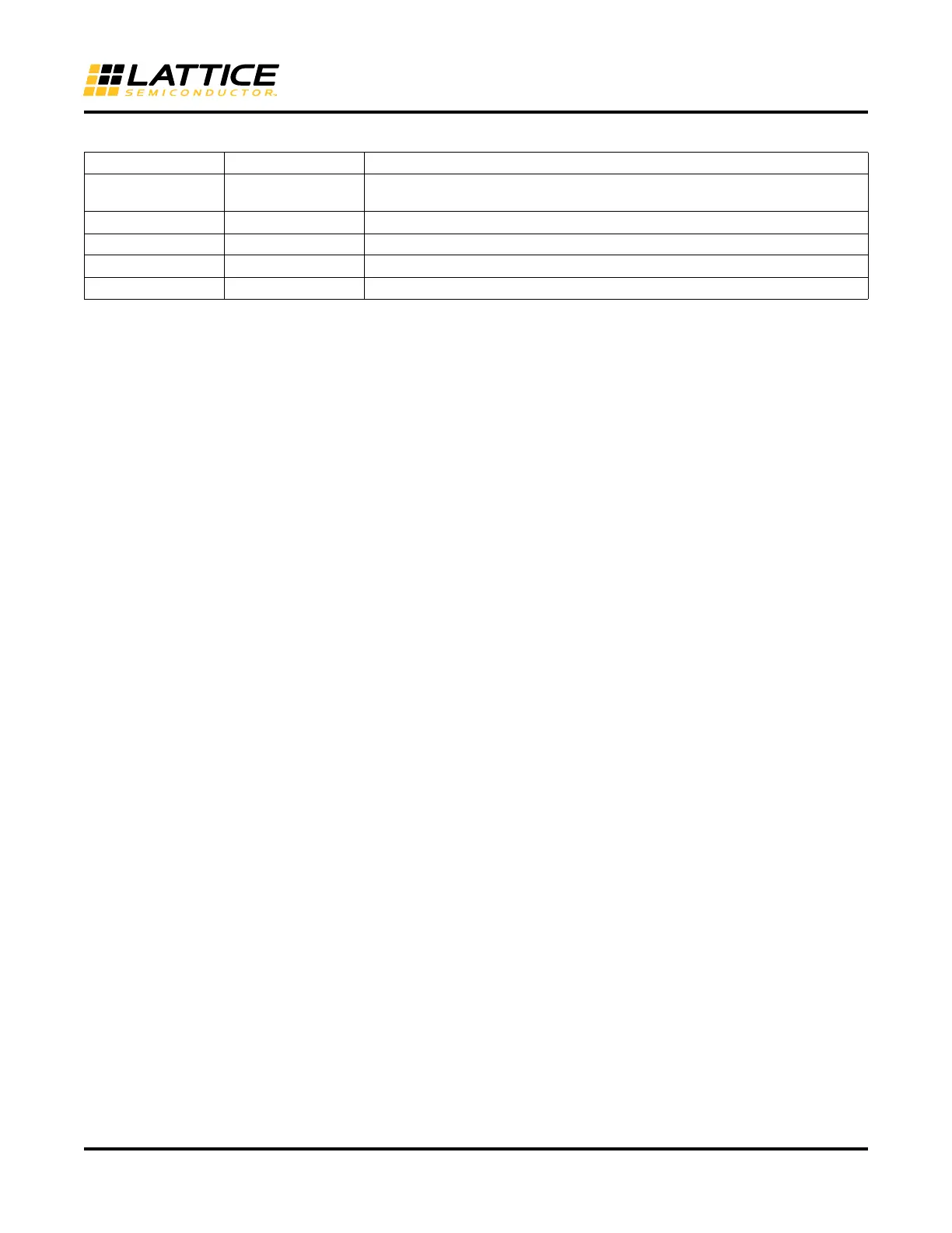
Table 27. ODDR71B Port List
Memory DDR Primitives
This section describes the primitives used to build DDR2, DDR3, DDR3L, LPDDR2 and LPDDR3 memory inter-
faces.
DQSBUF (DQS Strobe Control Block)
DQSBUF block is used to delay the incoming DQS signal by 90degrees. DQSBUF receives a delay code from
DDRDLL and shifts the signal accordingly. There will be one DQSBUF block for every 16 I/Os. The DQSBUF
should be used when the DQS clock tree is used for clocking the IDDR module.
The following describes the functions of the DQSBUF module:
• Receives the delay code from the DDRDLL and generates the 90 delayed DQS signal that is used as a Write
clock in the IDDR module
• User can choose to move the delay up or down using the dynamic margin control signals (loadn, move and direc-
tion).
• When this margin control circuit is used and LOADN goes high any further delay code changes from the
DDRDLL will not be reflected in the delay DQS signal. A soft IP is required to detect the code changes from the
DDRDLL and update the MOVE pulse input to the DQSBUF so that the DDRDLL code changes can be tracked.
• If margin control is not used then LOADN should be low to continuously get code from DDRDLL.
• Pause should be asserted prior to changing readclksel, DYNDEL<> or DLL code update.
• Receives READ clock select signals that are used to correctly position the READ signal with respect to the DQS
preamble
• Generates a BURSTDET output that can be used to validate the READ pulse positioning.
• Generates the Read and Write pointers required in the IDDR to correctly transfer data between the DQS and
ECLK clock domains
• Generates DQS write clocks to be used in ODDR modules to generate DQ and DQS
• Generates the Write Leveling delay required for DDR3 or LPDDR3 interfaces
DQSBUFM
DQSBUFM element is used for all the DDR Memory interfaces.
Port I/O Description
D0, D1, D2, D3, D4,
D5, D6
I Parallel data input to the ODDR (D0 is sent out first and D6 last)
ECLK I ECLK input (3.5x speed of SCLK)
SCLK I SCLK input
RST I Reset input
Q O DDR data output on both edges of ECLK
 Loading...


