60
ECP5 and ECP5-5G High-Speed I/O Interface
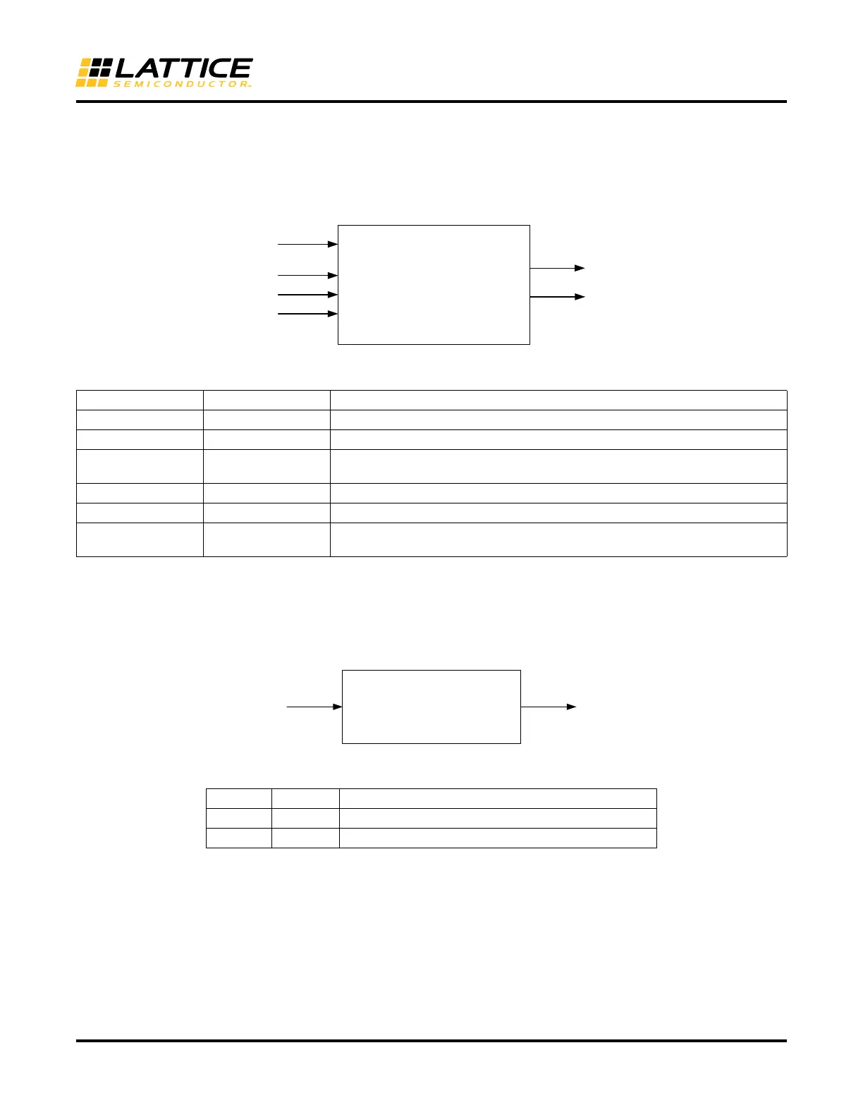
DELAYF
By default, the DELAYF is configured to factory delay settings based on the clocking structure. Users can overwrite
the DELAY setting using the MOVE and DIRECTION control inputs. The LOADN will reset the delay back to the
default value.
Figure 51. DELAYF Primitive
Table 15. DELAYF Port List
DELAYG
By default, the DELAYG will be configured to factory delay settings based on the clocking structure. Users cannot
change the delay when using this module.
Figure 52. DELAYG Primitive
Table 16. DELAYG Port List
Port I/O Description
A I Data input from pin or output register block
LOADN I ‘0’ on LOADN will reset to default delay setting
MOVE I
“Pulse” on MOVE will change delay setting. DIRECTION will be sampled at fall-
ing edge of MOVE.
DIRECTION I ‘1’ to decrease delay and ‘0’ to increase delay
Z O Delayed data to input register block or to pin
CFLAG O
Flag indicating the delay counter has reached the max (when moving up) or min
(when moving down) value
Port I/O Description
A I Data input from pin or output register block
Z O Delayed data to input register block or to pin
Z
A
DELAYF
LOADN
MOVE
DIRECTION
Z
CFLAG
Z
A
DELAYG
Z
 Loading...


