69
ECP5 and ECP5-5G High-Speed I/O Interface
Memory Input DDR Primitives
The following are the primitives used to implement various memory DDR input configurations.
IDDRX2DQA
This primitive is used to implement the DDR2 memory input interface at higher speeds and DDR3 memory inter-
face.
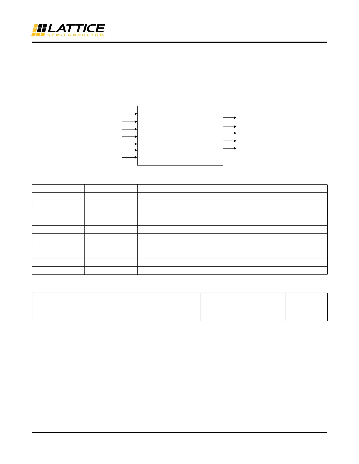
Figure 62. IDDRX2DQA Primitive
Table 31. IDDRX2DQA Port List
Table 32. Memory Primitive Attributes
Port I/O Description
D I DDR data input
RST I Reset to DDR registers
DQSR90 I DQS clock Input
ECLK I Fast edge clock
SCLK I Primary clock input (divide-by-2 of ECLK)
RDPNTR[2:0] I Read pointer from the DQSBUF module used to transfer data to ECLK
WRPNTR[2:0] I Write pointer from the DQSBUF module used to transfer data to ECLK
Q0, Q2 O Data at positive edge of DQS
Q1, Q3 O Data at negative edge of DQS
QWL O Data output used for write leveling
Attribute Description Values Default Valid Primitives
REGSET Set the Tristate register to either “SET” or
“RESET”. By Default value is “SET” so that
all output buffers are tristated by default
SET, RESET SET TSHX2DQA
SCLK
D
Q0
Q1
RST
ECLK
Q2
Q3
IDDRX2DQA
RDPNTR[2:0]
WRPNTR[2:0]
DQSR90
QWL
 Loading...


