16
ECP5 and ECP5-5G High-Speed I/O Interface
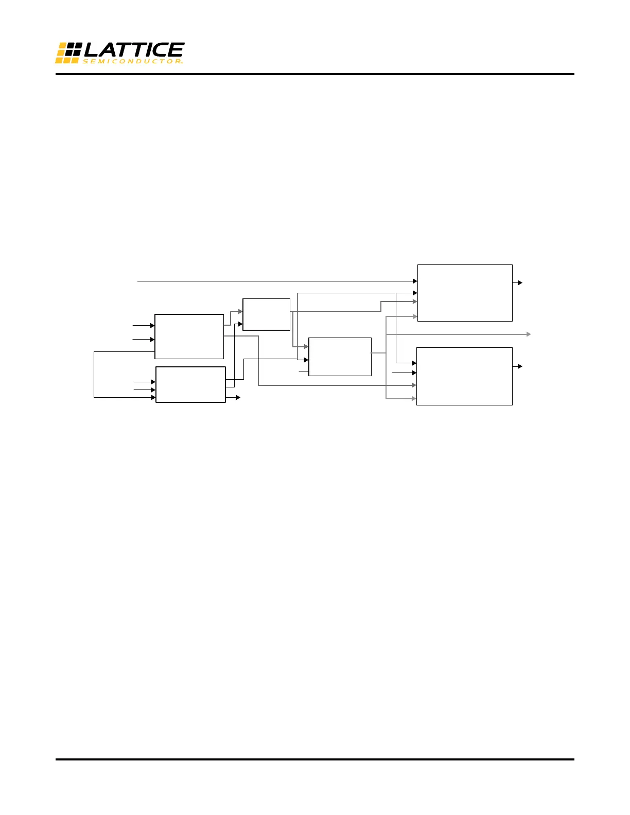
• The same ECLK and SCLK are used for both Data and Clock generation.
• The EHXPLLL element is used to generate the clocks for the data and clock ODDR modules. The clock used to
generate the clock output is delayed 90 to center to data at the output.
• The startup synchronization soft IP (GDDRX_SYNC) is required for this interface to tolerate the skew between
the ECLKSYNCB Stop input and the Reset to the DDR and CLKDIV modules.
• Optionally the user can choose to use the DELAYG or DELAYF element to delay the data output
• The output data can be optionally tristated using either a Tristate input going through an I/O register.
• The ECLKBRIDGE can be optionally enabled if the data bus will be crossing over between the left and right sides
of the device. If ECLKBRIDGE is enabled then the ECLKBRIDGECS element should be used in the interface
before the ECLKSYNCB element. This element can be enabled through Clarity Designer.
Figure 17. GDDRX2_TX.ECLK.Centered Interface
Interface Requirements
• The SCLK input to the output DDR modules must be routed on the primary clock tree and the ECLK input is
routed on the edge clock tree
• “USE PRIMARY” preference may be assigned to the SCLK net
• The user must set the timing preferences as per section “Timing Analysis Requirement”
GDDRX71_TX.ECLK
This interface is used to implement transmit side of the 7:1 LVDS interface DDR using the 7 to 1 gearing with
ECLK. The clock output is aligned to the data output.
This DDR interface uses the following modules:
• ODDRX71B is used to generate the data output
• The high speed ECLK is routed to the edge clock tree through the ECLKSYNCB module
• The SCLK is routed on the primary clock tree and is generated from the ECLK using the CLKDIVD module
• The same ECLK and SCLK are used for both Data and Clock generation.
• The startup synchronization soft IP (GDDRX_SYNC) is required for this interface to tolerate the skew between
the ECLKSYNCB Stop input and the Reset to the DDR and CLKDIV modules.
• The ECLKBRIDGE can be optionally enabled if the data bus will be crossing over between the left and right sides
of the device. If ECLKBRIDGE is enabled then the ECLKBRIDGECS element should be used in the interface
before the ECLKSYNCB element. This element can be enabled through Clarity Designer.
D[3:0]
SCLK
RST
Q
Data [3/ 7/ 9:0]
SCLK
RST
Q
“0101”
Refclk
Dout
Clkout
ECLK
CLKDIVF
CLKI
RST
ALIGNWD
CDIVX
D[3:0]
ECLK
ODDRX2F
Edge 1
Primary
Sclk
EHXPLLL
CLKOP
CLKI
RST
CLKOS
LOCK
1'b 0
Edge
2
ECLKI
STOP
ECLKO
ECLKSYNCB
Reset
GDDR_SYNC
Sync_clk
RST
START
SYNC_CLK
DDR _RESET
STOP
READY
Pll_reset
Ready
ODDRX2F
 Loading...


