9
ECP5 and ECP5-5G High-Speed I/O Interface
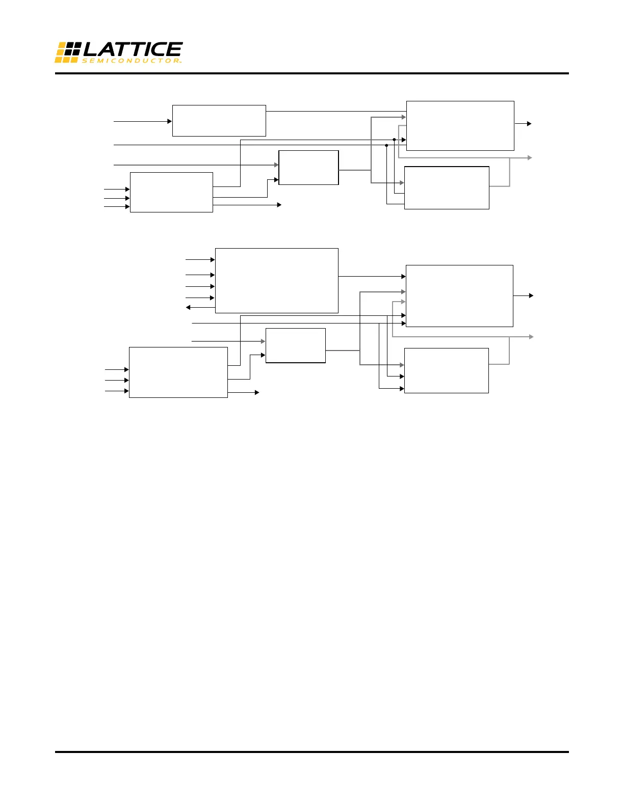
Figure 8. GDDRX2_RX.ECLK.Centered Interface (Static Delay)
Figure 9. GDDRX2_RX.ECLK.Centered Interface (Dynamic Data Delay)
Interface Requirements
• The clock input must use a PCLK input so that it can be routed directly to the edge clock tree.
• ECLK must use the Edge clock tree and the SCLK out of the CLKDIVF must use the Primary clock tree, software
will error out if these dedicated clock routes are not used
• “USE PRIMARY” preference may be assigned to the SCLK net
• The user must set the timing preferences as per section “Timing Analysis Requirement”
GDDRX2_RX.ECLK.Aligned
Generic Receive DDR with the 2X gearing with ECLK. Input Clock is coming in edge aligned to the Data. This inter-
face must be used for speeds above 20 MHz.
This DDR interface uses the following modules:
• IDDRX2F element for 2X mode to capture the data
• DDRDLLA/DLLDELD blocks are used to phase shift the incoming clock routed to the Edge clock (ECLK) clock
tree through the ECLKSYNCB module
• CLKDIVF module is used to divide the incoming clock by 2
• Static data delay element DELAYG to delay the incoming data enough to remove the clock injection time
• Optionally the user can choose to use Dynamic Data delay adjustment using DELAYF element to control the
delay on the DATA dynamically. DELAYF will also allow user to override the input delay set. The type of delay
required can be selected through Clarity Designer
ALIGNWD
Datain
Clkin
A
DELAYG
Z
ECLKI
STOP
ECLKO
SCLK
D
Q[3:0]
RST
ALIGNWD
ECLK
IDDRX2F
Edge
Primary
Sclk
CLKDIVF
CLKI
RST
CDIVX
AlignWD
Q[3:0]
ECLKSYNCB
DEL_MODE=
ECLK_CENTERED
sync_reset
GDDR _SYNC
Sync _clk
Start
RST
START
SYNC_CLK
DDR_RESET
STOP
READY
Ready
Data_LoadN
Data_Move
Data_Direction
A
DELAYF
LOADN
MOVE
DIRECTION
CFLAG
Datain
Data_CFlag
Z
ECLKI
STOP
ECLKO
SCLK
D
RST
ALIGNWD
ECLK
Edge
Primary
Sclk
CLKDIVF
CLKI
RST
ALIGNWD
CDIVX
AlignWD
Clkin
Q[3:0]
Q[3:0]
IDDRX2F
ECLKSYNCB
sync_reset
GDDR_SYNC
Sync_clk
Start
RST
START
SYNC_CLK
DDR_RESET
STOP
READY
Ready
DEL_MODE=
ECLK_CENTERED
 Loading...


