68
ECP5 and ECP5-5G High-Speed I/O Interface
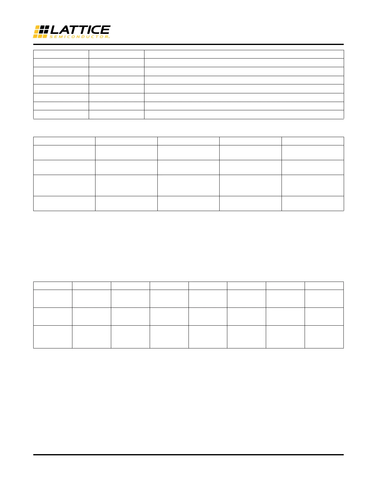
Table 29. DQSBUFM Attributes
Input and Output Memory DDR Primitives
The ECP5 and ECP5-5G device IDDR/ODDR modules support 4:1(2X) gearing mode that are used to implement
the memory functions.
Table 30 shows a summary of all the DDR memory primitives. See the sections below for detailed descriptions.
Table 30. Summary of all DDR Memory Primitives
DQSR90 O 90° delay DQS used for read
DQSW270 O 90° delay clock used for DQ write
DQSW O Clock used for DQS write
RDPNTR[2:0] O Read pointer for IFIFO module
WRPNTR[2:0] O Write pointer for IFIFO module
DATAVALID O Signal indicating start of valid data
BURSTDET O Burst Detect indicator
Attribute Description Values Default DQSBUF
DQS_LI_DEL_ADJ Sign bit for READ delay
adjustment, DDR input
PLUS, MINUS PLUS
All
DQS_LI_DEL_VA Value of delay for input
DDR.
0 to 255(PLUS)
1 to 256 (MINUS)
Note
1
All
DQS_LO_DEL_ADJ Sign bit for WRITE
delay adjustment, DDR
output
PLUS, MINUS PLUS
All
DQS_LO_DEL_VAL Value of delay for output
DDR.
0 to 255 (PLUS)
1 to 256 (MINUS)
Note
1
All
1. Default value is set based on device characterization to achieve the 90 degree phase shift
DDR Memory DQ Input DQ Output DQ Tristate DQS Output DQS Tristate Addr/Cmd Clock
DDR2
DDR3
DDR3L
IDDRX1DQA ODDRX2DQA TSHX2DQA ODDRX2DQSB TSHX2DQSA
ODDRX1F
CS_N:
OSHX2A
ODDRX2F
LPDDR2
IDDRX2DQA ODDRX2DQA TSHX2DQA ODDRX2DQSB TSHX2DQSA
ODDRX2DQA
CS_N & CKE:
ODDRX2DQA
1
ODDRX2DQSA
LPDDR3
IDDRX2DQA ODDRX2DQA TSHX2DQA ODDRX2DQSB TSHX2DQSA
ODDRX2DQA
CS_N, CKE &
ODT:
ODDRX2DQA
1
ODDRX2DQSA
Note: The D0 and D1 inputs are tied together. The D2 and D3 inputs are also tied together.
Port I/O Description
 Loading...


