72
ECP5 and ECP5-5G High-Speed I/O Interface
Table 36. TSHX2DQSA Port List
Memory Output DDR Primitives for Address and Command
The following are the primitives used to implement the address and command outputs to the DDR memory.
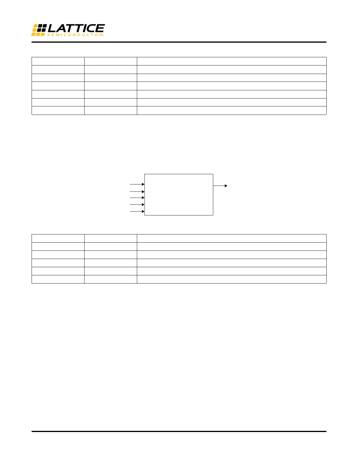
OSHX2A
This primitive is used to generate the address and command for DDR3 memory with x2 gearing and write leveling.
Figure 67. OSHX2A Primitive
Table 37. OSHX2A Port List
Port I/O Description
T0, T1 I Tristate input (T0 is output first then T1)
ECLK I ECLK input (2x speed of SCLK)
SCLK I SCLK input
DQSW I DQSW includes write leveling phase shift from ECLK
RST I Reset Input
Q O Tristate output
Port I/O Description
D0, D1 I Data input (D0 is output first then D1)
ECLK I ECLK input (2x speed of SCLK)
SCLK I SCLK input
RST I Reset input
Q O Address and command output
 Loading...


