59
ECP5 and ECP5-5G High-Speed I/O Interface
DDR Software Primitives and Attributes
This section describes the software primitives that can be used to implement all the DDR interfaces. These primi-
tives are divided into ones that are used to implement the DDR data and ones for DDR Strobe signal or the Source
Synchronous clock. The DQSBUF primitives are used to generate the signals required to correctly capture the data
from the DDR memory.
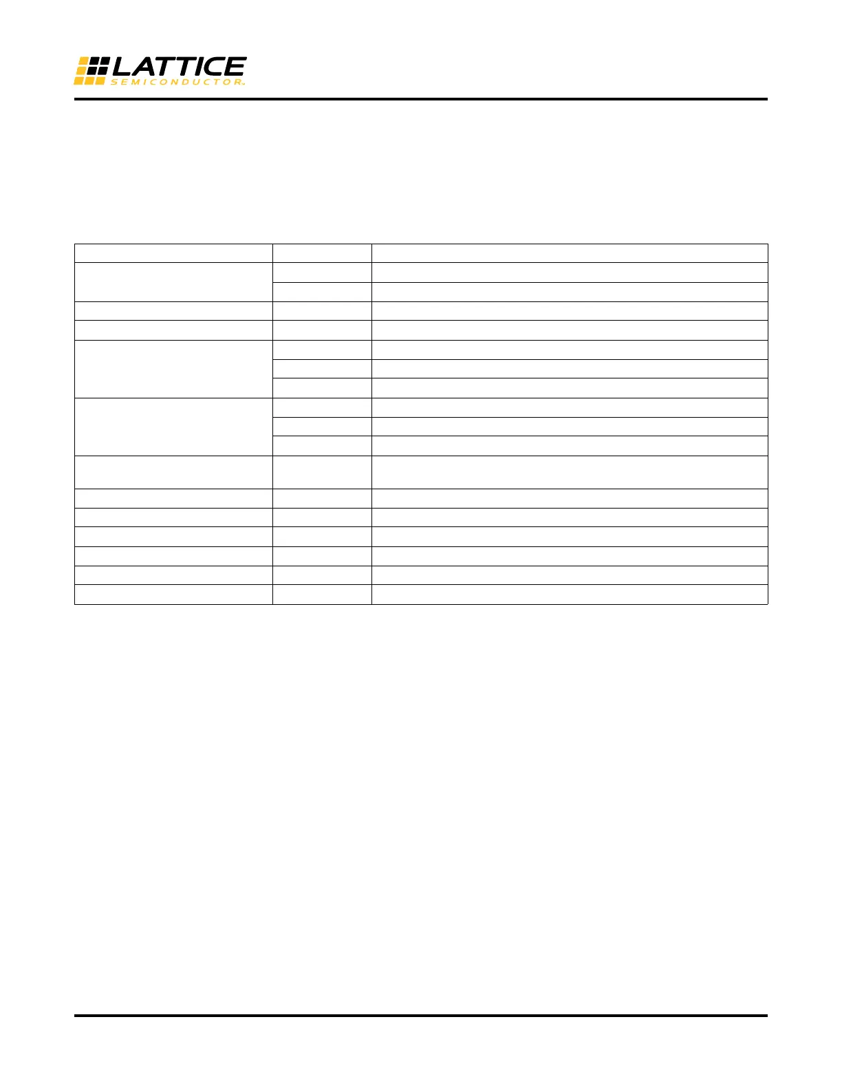
Table 14. Software Primitives
Input/Output DELAY
The DELAY block can be used to delay the input data from the input pin to the IDDR or IREG or FPGA OR to delay
the output data from the ODDR, OREG or FPGA fabric to the output pin. It is useful to adjust for any skews
amongst the input or output data bus. It can also be used to generate skew between the bits of output bus to
reduce SSO noise.
The DELAY block can be used with IDDR or ODDR modules, SDR module, as well as on the direct input to the
FPGA. The DELAY is shared by the input and output paths and hence can only be used either to delay the input
data or the output data on a given pin.
The data input to this block can be delayed using:
• Pre-determined delay value (for Zero Hold time, delay based on Interface Type)
• Fixed Delay values entered by the user
The data input to this block can also be dynamically updated using counter up and down controls. You can option-
ally bypass the DELAY block completely as well.
Type Primitive Description
Input or Output Delay DELAYF Dynamic Delay module
DELAYG Static Delay module, used to remove clock injection time
DDRDLL DDRDLLA DLL used to generate 90 degree phase shift
DLL Delay DLLDELD Slave Delay module used for Generic DDR
Generic DDR Data Input IDDRX1F Generic DDR 1X gearing registers
IDDRX2F Generic DDR 2X gearing registers
IDDR71B Generic DDR 7:1 gearing registers, shared by two IOLOGIC blocks
Generic DDR Data Output ODDRX1F Generic DDR 1X gearing registers
ODDRX2F Generic DDR 2X gearing registers
ODDR71B Generic DDR 7:1 gearing registers, shared by two IOLOGIC blocks
DDR Memory DQSBUF Control DQSBUFM Used to phase shift DQS Strobe signal and generate control signals for
DDR memory
DDR Memory DQ Input IDDRX2DQA Used to receive DQ input
DDR Memory DQ Output ODDRX2DQA Used to transmit DQ output
DDR Memory DQS Output ODDRX2DQSB Used to transmit DQS output
DDR Memory Data Tristate TSHX2DQA Used for DQ Tristate output
DDR Memory DQS Tristate TSHX2DQSA Used for DQS Tristate output
DDR Memory Address/Command OSHX2A Used to generate the Address/Command output
 Loading...


