27
ECP5 and ECP5-5G High-Speed I/O Interface
Features for Memory Interface Implementation
The ECP5 and ECP5-5G devices contain a variety of features to simplify implementation of the read and write
operations of a DDR interface:
• DQS Clock Tree spanning the DQS group
• DDRDLL used to generate the 90 degree delay codes
• DLL-compensated DQS delay elements
• Input FIFO for read data clock domain transfer
• Dedicated DDR Memory input and output registers
• Dynamic Margin Control Circuit to adjust Read and Write delays
• Input/Output Data Delay used to compensate for DQS clock tree delay
DQS Grouping
In DDR interfaces with eight DQ pads associated to one DQS pad, each DQS group generally consists of at least
10 I/Os (one DQS, eight DQ and one DM) for an 8-bit DDR2 memory interface or 11 I/Os (two DQS, eight DQ, one
DM) to implement a complete 8-bit DDR3/DDR3L/LPDDR2/LPDDR3 memory interface. In case of LPDDR2/3, two
additional DQS groups are required to generate the CA[9:0] (with 10 I/Os) and Control/CLKP/CLKN (with 5 I/Os for
LPDDR3 and 4 I/O on LPDDR2) outputs.
In ECP5 and ECP5-5G devices, a DQS group consists of 12 to 16 I/Os depending on the device and package
selected to accommodate these DDR interface needs. ECP5 and ECP5-5G devices support DQS signals on the
left and right sides of the device.
Each DQS signal spans across 12 to 16 I/Os. Any 10 (for DDR2) or 11 (for DDR2/DDR3/LPDDR2/LPDDR3) of
these 16 I/Os spanned by the DQS can be used to implement an 8-bit Data side interface. For LPDDR2/LPDDR23,
any group with 10 I/Os is required for CA[9:0] bus and another group with 5 I/Os for LPDDR3 and 4 I/Os for
LPDDR2 is required to generate the Control and CLKP/CLKN outputs. In addition to the DQS grouping, the user
must also assign the reference voltage (VREF) input to an I/O in that bank required to implement the referenced I/O
standard.
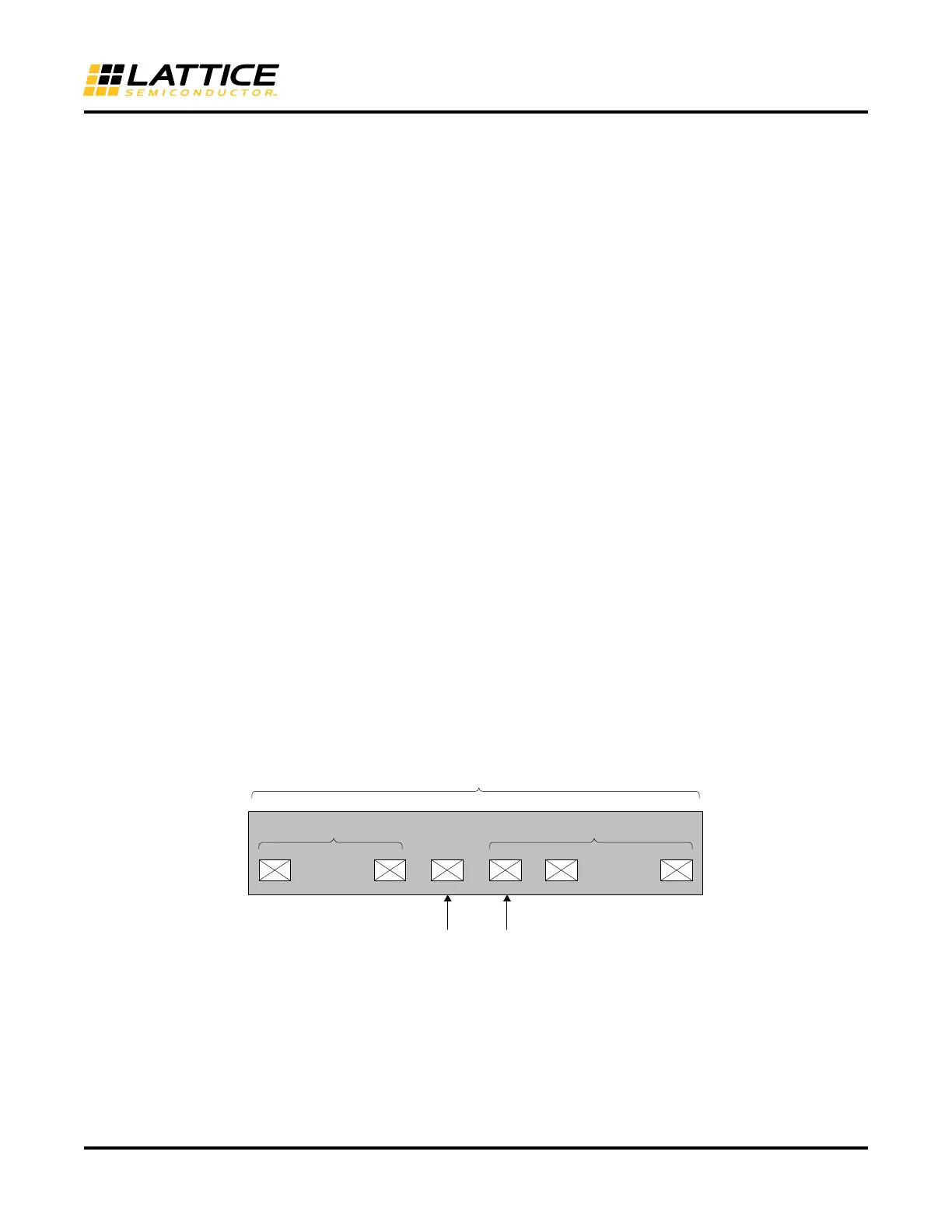
Figure 28. DQ-DQS Grouping
Figure 28 shows a typical DQ-DQS group for ECP5 and ECP5-5G devices. The 10th I/O Pad of this 16 I/O group is
the dedicated DQS pin. All the 9 pads before the DQS and 6 pads after the DQS are covered by this DQS bus
span. If a differential DQS pair is required then the 11th pad is used by the DQS# signal. The user can assign any
other I/O pads to be DQ data or DM pins. Therefore, for example, to implement a 32-bit wide memory interface you
would need to use four such DQ-DQS groups when eight-to-one DQ-DQS association is used.
In case of LPDDR2 and LPDDR2, two additional DQS groups are required to assign the CA[9:0] and the control
signals.
DQS PAD (10
th
pad)
16 I/ O PADS
DQ , DM DQ , DM
- - - - - -
DQS# PAD (11
th
pad)
 Loading...


