13
ECP5 and ECP5-5G High-Speed I/O Interface
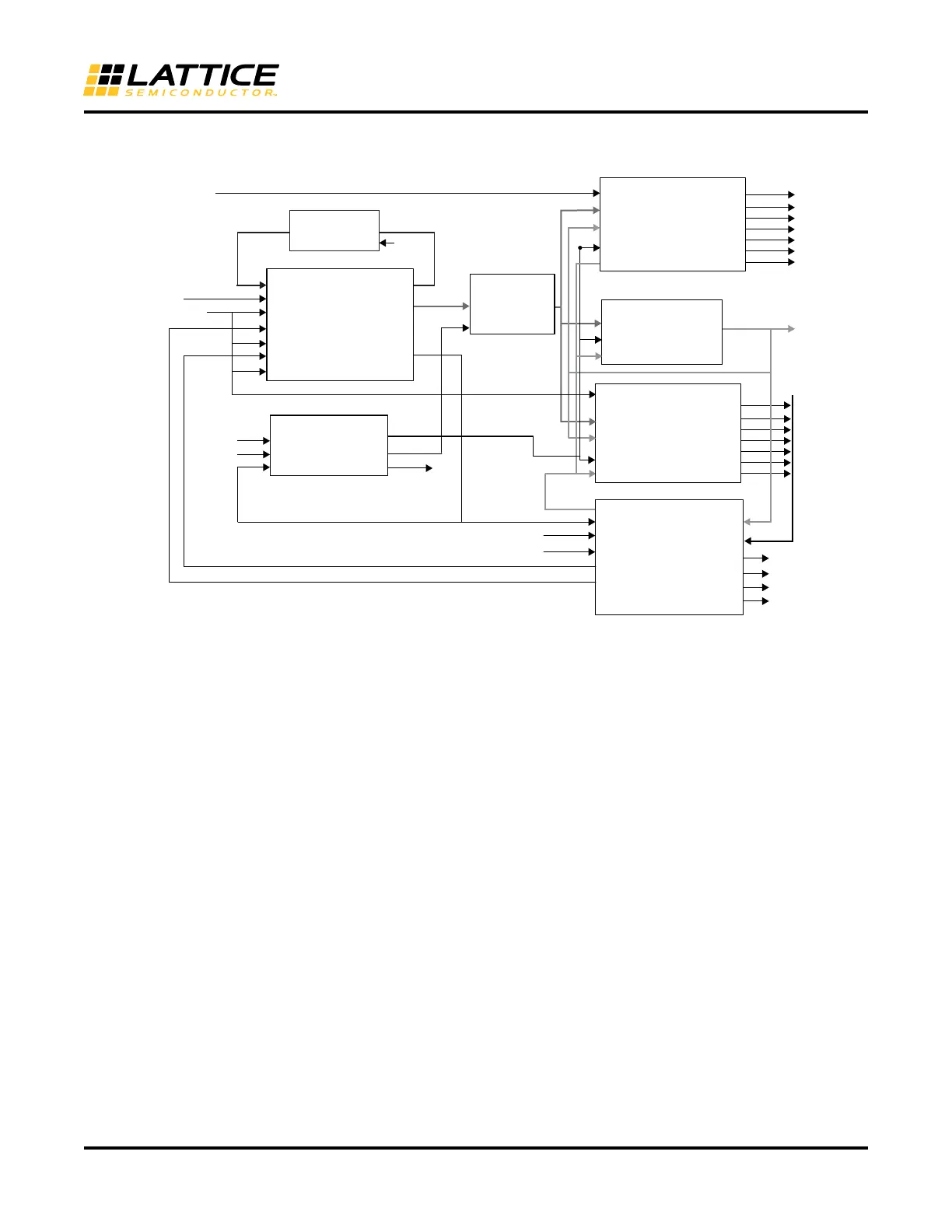
The following figures show the interface with the soft IP modules.
Figure 13. GDDRX71_RX.ECLK Interface
Interface Requirements
• The clock input must use a dedicated PLL input pin so it is routed directly to the PLL
• CLKOP output of the PLL must be used as feedback using another edge clock tree to compensate for ECLK tree
delay used by CLKOS. Hence this interface will use two ECLK trees.
• ECLK must use the Edge clock tree and the SCLK out of the CLKDIVF must use the Primary clock tree.
• “Use Primary” preference may be assigned to the SCLK out of the CLKDIVF module
GDDRX1_TX.SCLK.Aligned
This interface is used to implement Generic Transmit DDR with 1X gearing using primary clock (SCLK). The Clock
output is aligned to the Data output.
This DDR interface uses the following modules:
• ODDRX1F element is used to generate the data output
• The primary clock (SCLK) is used as the clock for both data and clock generation
• Optionally the user can choose to use the DELAYG or DELAYF element to delay the output data
• The output data can be optionally tristated using either a Tristate input going through an I/O register.
Datain
Clkin
EHXPLLL
CLKOP
CLKI
PHASESEL
PHASEDIR
RST
ECLKI
STOP
ECLKO
Edge
Primary
sclk
CLKDIVF
CLKI
RST
ALIGNWD
CDIVX
(divby 3.5)
CLKFB
CLKOS
LOCK
PHASESTEP
SCLK
D
Q
0
Q
1
RST
ALIGNWD
ECLK
Q
2
Q
3
Q
4
Q
5
Q
6
IDDR71B
SCLK
DQ0
Q1
RST
ALIGNWD
ECLK
Q2
Q3
Q4
Q5
Q6
IDDR 71 B
Q[0]
Q[1]
Q[2]
Q[3]
Q[4]
Q[5]
Q[6]
Edge
ECLKSYNCB
clock
_
phase [ 6 :0 ]
pll _reset
Sync_reset
GDDR _SYNC
Sync_clk
RST
START
SYNC_CLK
DDR_RESET
STOP
READY
Ready
RX_ SCLK
RXCLK_
WORD
<6:0>
UPDATE
PLL_LOCK
RST
PHASESTEP
PHASEDIR
ALIGNWORD
WINDOW_SIZE
BIT_ LOCK
WORD_LOCK
READY
Align_ready
Update
Bw_align_Rst
Window_size
Bit_lock
Word_lock
ECLKI
STOP
ECLKO
ECLKSYNCB
“0”
PHASELOADREG
“1”
 Loading...


