67
ECP5 and ECP5-5G High-Speed I/O Interface
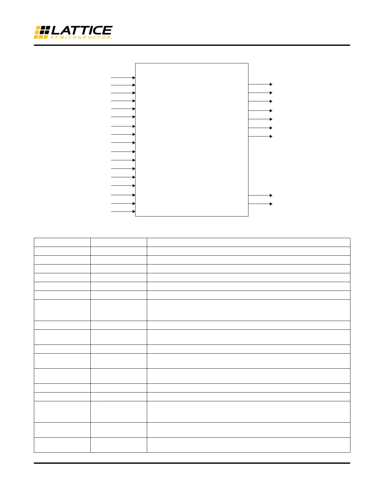
Figure 61. DQSBUFM Primitive
Table 28. DQSBUF Port List
Port I/O Description
DQSI I DQS input from the DQS pin
DDRDEL I Delay code from DDRDLL
ECLK I Edge clock
SCLK I System clock
RST I Reset input
READ[1:0] I Read input width for DQSBUFM
READCLKSEL0,
READCLKSEL1,
READCLKSEL2
I Read clock pulse selection
DYNDELAY[7:0] I Dynamic Write leveling delay (only for DDR3)
PAU SE I
Pause input to stop the DQSW/DQSW270 during write leveling or DDRDLL delay
code change.
RDLOADN I Used to reset back to 90° delay for read side DQS
RDMOVE I
Pulse is required to change delay settings. The value on Direction will be sam-
pled at “falling edge” of MOVE. Used to change delay on the read side DQS.
RDDIRECTION I
Indicates delay direction. ‘1’ decreases the delay count, ‘0’ increases the delay
count. Used to change delay on the read side DQS.
RDCFLAG O Indicates the delay counter has reached max value for the read side DQS delay.
WRLOADN I Used to reset back to 90° delay for write side DQSW270
WRMOVE I
Pulse is required to change delay settings. The value on Direction will be sam-
pled at the falling edge of MOVE. Used to change delay on the write side
DQSW270.
WRDIRECTION I
Indicates delay direction. ‘1’ decrease delay count, ‘0’ increases the delay count.
Used to change delay on the write side DQSW270.
WRCFLAG O
Indicates the delay counter has reached the maximum value for the write side
DQSW270 delay.
DQSBUFM
DQSI
DQSR90
DQSW
DATAVALID
DDRDEL
READ [1:0]
ECLK
WRPNTR[2:0]
RDPNTR[2:0]
SCLK
RST
DYNDELAY
[7:0]
READCLKSEL0
BURSTDET
DQSW270
READCLKSEL1
READCLKSEL2
RDLOADN
RDMOVE
RDDIRECTION
RDCFLAG
WRLOADN
WRMOVE
WRDIRECTION
WRCFLAG
PAUSE
 Loading...


