65
ECP5 and ECP5-5G High-Speed I/O Interface
Table 25. ODDRX1F Port List
ODDRX2F
This primitive is used to receive Generic DDR with 2X gearing.
Figure 59. ODDRX2F
Table 26. ODDRX2F Port List
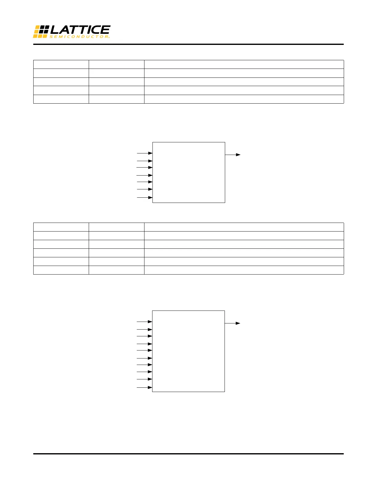
ODDR71B
This primitive is used for 7:1 LVDS ODDR implementation.
Figure 60. ODDR71B Primitive
Port I/O Description
D0, D1 I Parallel data input to ODDR (D0 is sent out first then D1)
SCLK I SCLK input
RST I Reset input
Q O DDR data output on both edges of SCLK
Port I/O Description
D0, D1, D2, D3 I Parallel Data input to the ODDR (D0 is sent out first and D3 last)
ECLK I ECLK input (2x speed of SCLK)
SCLK I SCLK input
RST I Reset input
Q O DDR data output on both edges of ECLK.
D0
D1
SCLK
RST
Q
ODDRX2F
D2
D3
ECLK
D0
D1
SCLK
RST
Q
ODDR71B
D2
D3
ECLK
D4
D5
D6
 Loading...


