MachXO2 and MachXO3 Starter Kit Evaluation Board User Guide
Evaluation Board User Guide
© 2014-2022 Lattice Semiconductor Corp. All Lattice trademarks, registered trademarks, patents, and disclaimers are as listed at www.latticesemi.com/legal.
All other brand or product names are trademarks or registered trademarks of their respective holders. The specifications and information herein are subject to change without notice.
4 FPGA-EB-02036-1.4
Figures
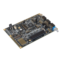
Figure 2.1. MachXO3 Board (MachXO3L Version), Top Side ................................................................................................ 7
Figure 2.2. MachXO3 Board (MachXO3L Version), Bottom Side .......................................................................................... 8
Figure 7.1. MachXO2 and MachXO3L/LF-6900C Block Diagram ......................................................................................... 12
Figure 6.1. Demonstration Design Block Diagram .............................................................................................................. 13
Figure 7.2. J3/J4 Header Landing Callout ............................................................................................................................ 22
Figure 7.3. J6/J8 Header Landing Callout ............................................................................................................................ 22
Figure 7.4. J1 Header Landing and LED Array Callout ......................................................................................................... 23
Figure A.1. Block Diagram ................................................................................................................................................... 29
Figure A.2. USB Interface to JTAG ....................................................................................................................................... 30
Figure A.3. FPGA ................................................................................................................................................................. 31
Figure A.4. FPGA ................................................................................................................................................................. 32
Figure A.5. Power LEDs ....................................................................................................................................................... 33
Figure A.6. Bank 2 I/O ......................................................................................................................................................... 34
Figure A.7. Bank 3, 4, 5 I/O ................................................................................................................................................. 35
Figure A.8. Power Decoupling and LEDs ............................................................................................................................. 36
Tables
Table 7.1. Starter Kit Components and Interfaces .............................................................................................................. 13
Table 6.1. DIP Switch and LED Behavior ............................................................................................................................. 14
Table 7.2. Expansion Connector Reference ........................................................................................................................ 17
Table 7.3. Expansion Header Pin Information (J3) .............................................................................................................. 18
Table 7.4. Expansion Header Pin Information (J4) .............................................................................................................. 19
Table 7.5. Expansion Header Pin Information (J6) .............................................................................................................. 20
Table 7.6. Expansion Header Pin Information (J8) .............................................................................................................. 21
Table 7.7. MachXO2 and MachXO3 FPGA Interface Reference .......................................................................................... 23
Table 7.8. USB/JTAG Interface Reference ........................................................................................................................... 23
Table 7.9. JTAG Programming Pin Information ................................................................................................................... 24
Table 7.10. SPI Programming Pin Information .................................................................................................................... 24
Table 7.11. I
2
C Programming Pin Information .................................................................................................................... 24
Table 7.12. Power and User LEDs Reference ...................................................................................................................... 24
Table 7.13. USB Interface Reference .................................................................................................................................. 25
Table 9.1. Ordering Information ......................................................................................................................................... 27