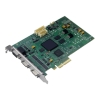
98 Appendix B: Technical information
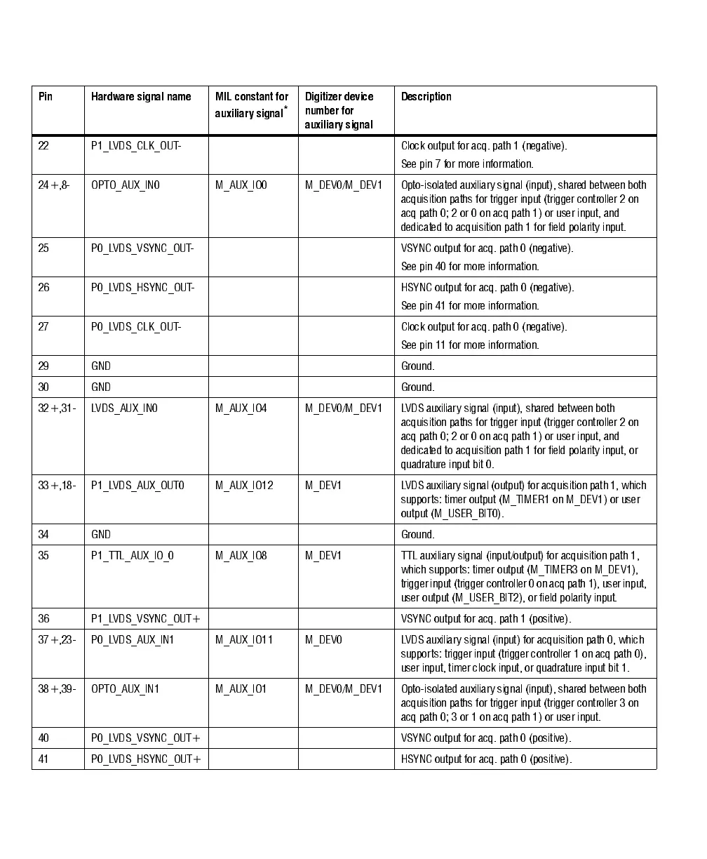
22 P1_LVDS_CLK_OUT- Clock output for acq. path 1 (negative).
See pin 7 for more information.
24+,8- OPTO_AUX_IN0 M_ AUX_IO0 M_DEV0/M_DEV1 Opto-isolate d auxiliary signal (inp ut), share d between both
acquisition paths for trigger input (trigger controller 2 on
acq path 0; 2 or 0 on acq path 1) or user input, and
dedicated to acquisition path 1 for field polarity input.
25 P0_LVDS_VSYNC_OUT- VSYNC output for acq. path 0 (negative).
See pin 40 for more information.
26 P0_LVDS_HSYNC_OUT- HSYNC output for acq. path 0 (negative).
See pin 41 for more information.
27 P0_LVDS_CLK_OUT- Clock output for acq. path 0 (negative).
See pin 11 for more information.
29 GND Ground.
30 GND Ground.
32+,31- LVDS_AUX_IN0 M_AUX_IO4 M_DEV0/M_DEV1 LVDS auxiliary signal (input), shared between both
acquisition paths for trigger input (trigger controller 2 on
acq path 0; 2 or 0 on acq path 1) or user input, and
dedicated to acquisition path 1 for field polarity input, or
quadrature in put bit 0.
33+,18- P1_ LVDS_AUX_OUT0 M_ AUX_IO12 M_ DEV1 LVDS auxiliary signal (output) for acqui sition path 1, which
supports: timer output (M_TIMER1 on M_DEV1) or user
output (M_USER_BIT 0).
34 GND Ground.
35 P1_TTL_AUX_IO_0 M_AUX_IO8 M_DEV1 TTL auxiliary signal (input/output) for acquisition path 1,
which supports: timer output (M_TIMER3 on M_DEV1),
trigger in put (tri gge r controller 0 on acq path 1), use r i nput,
user output (M_USER_BIT2), or field polarity input.
36 P1_LVDS_VSYNC_OUT+ VSYNC output for acq. path 1 (positive).
37+,23- P0_LVDS_AUX_IN1 M_AUX_IO11 M_DEV0 LVDS auxiliary signal (input) for acquisition path 0, which
supports: trigger input (trigger controller 1 on acq path 0),
user input, timer clock input, or quadrature input bit 1.
38+,39- OPTO_AUX_IN1 M_AUX_IO1 M_DEV0/M_DEV1 Opto-isolate d auxiliary signal (inp ut), share d between both
acquisition paths for trigger input (trigger controller 3 on
acq path 0; 3 or 1 on acq path 1) or user input.
40 P0_LVDS_VSYNC_OUT+ VSYNC output for acq. path 0 (positive).
41 P0_LVDS_HSYNC_OUT+ HSYNC output for acq. path 0 (positive).
Pin Hardware signal name MIL constant for
auxiliary signal
*
Digitizer device
number for
auxiliary signal
Description