13. I
2
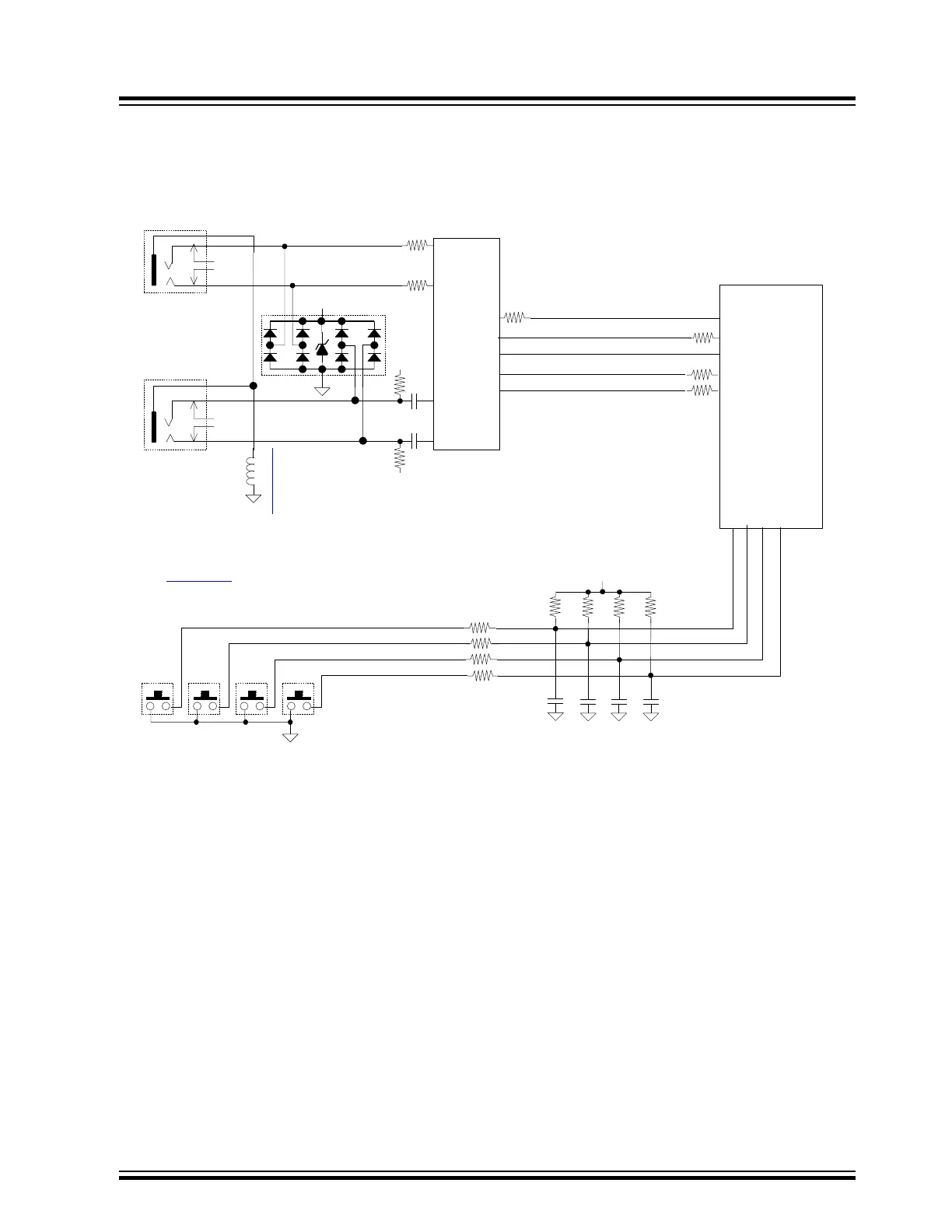
S and Push Button Protection Illustration
Figure 13-1. I
2
S and Push Button Protection Design Diagram
AUDIO HEADPHONE & MICROPHONE PROTECTION EXAMPLE
D5V0P4UR6SO
2
1
3
4
5
6
Codec
HP / Line-Out
1
3 (Right)
5
4
2 (Left)
Mic / Line-In
1
5
4
3 (Right)
2 (Left)
NC
MPWR
Microphone Power
Pushbuttons
0.1uf
20k
VDD
0.1uf
20k
0.1uf
20k
0.1uf
20k
SwitchHDWDe-bounce & ESD protection
MCU
I/O
I/O
I/O
I/O
33
33
MCLK
BIT_CLK
LRCK
SDI
REFCLKx - MCKx
SCKx
SS#x - FSx
SDOx
Transient
Suppressors -->
NOTE:
The TVS ground MUST be tied directly to ground
plane not to a ground trace to minimize inductance.
NOTE:
Ground connection on all TVS MUST be directly connected to ground
plane and not through a trace to ground to minimize inductance. In
addition, they should be located as close to the external audio jacks
connectors and switches as possible
MI1206L501R-10
MI0805J102R-10
1kΩ @ 100MHz, DCR=0.15Ω(max), 1A
1k
1k
1k
1k
33
SDO
33
SDIx
Signal naming:
PIC32MX/MM/MZ/MK – SAM/PIC32C
13.1 Key I
2
S and Push Button Protection Design Points
• Push Button 1k series resistors and 0.1 µF caps form an ESD RC low-pass filter and a hardware push button
denouncer
•
ESD protection on ground, audio in, and audio out signals
Return to Checklist
I2S and Push Button Protection Illustratio...
© 2022 Microchip T
echnology Inc.
and its subsidiaries
Manual
DS70005439B-page 57