17. Comprehensive PCB Layout Guidelines and Recommendations
1. Layout differential and high-speed traces first, maintaining differential impedance matching on PCB layer 1
adjacent to ground plane layer
.
2. Ensure that all clock and high-speed signal traces must have an unbroken reference ground plane with no
gaps or voids beneath them.
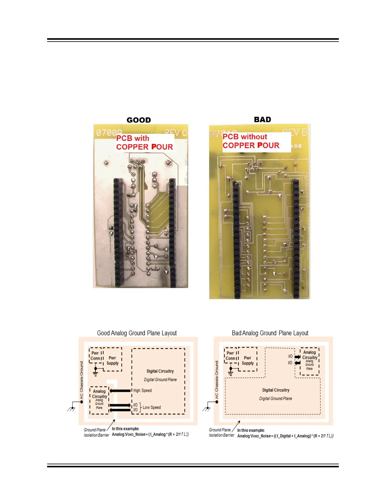
3. Copper pour all voids on signal layers with signal ground.
Figure 17-1. Copper Ground Pour in PCB Voids
4. Use separate digital and analog grounds when appropriate and do not connect the ground planes together
except at power ground (i.e., closest to the respective input power regulator).
Figure 17-2. Analog V
ersus Digital Ground Layout Placement
Comprehensive PCB Layout Guidelines and Recommenda...
© 2022 Microchip T
echnology Inc.
and its subsidiaries
Manual
DS70005439B-page 64