11.2 Ground Loops
Problem 26: There is intermittent data corruption on communication links between remote PCB stations or
equipment.
•
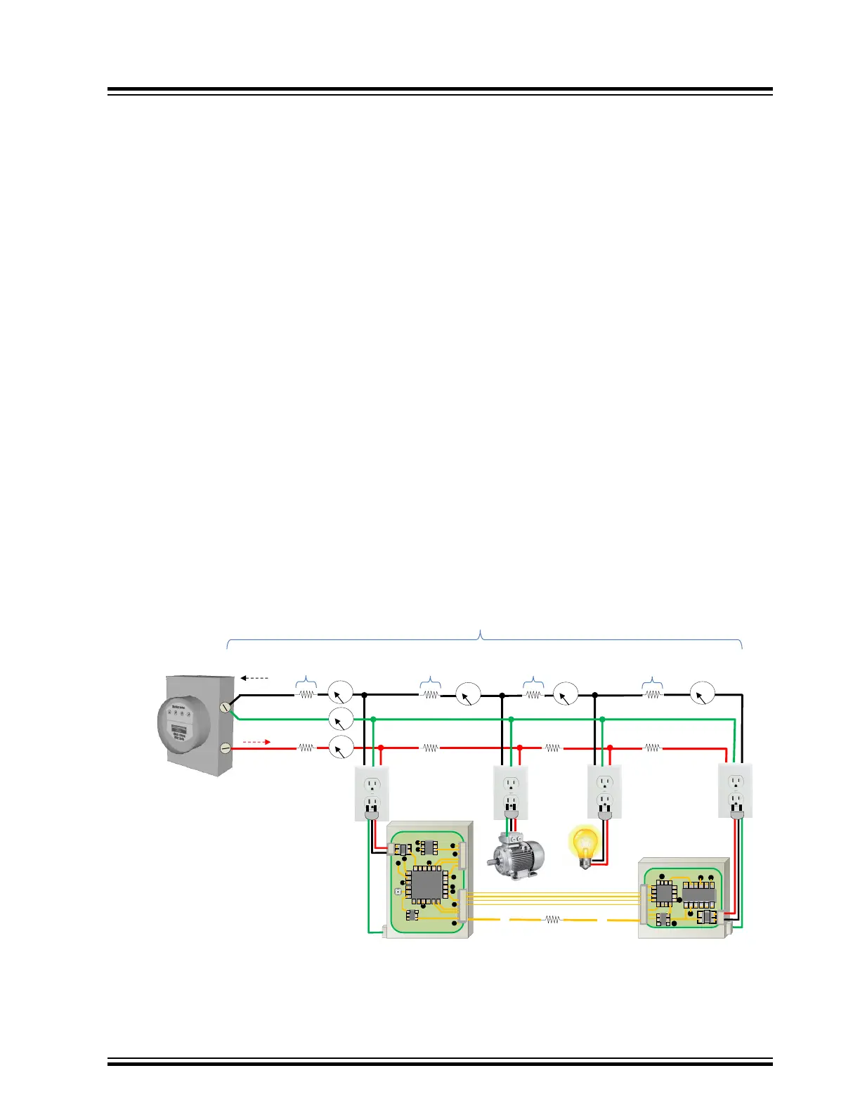
Ground loops can be caused when equipment between different locations are digitally interconnected through
cables sharing a common digital ground, but whose local PCB digital grounds are at different potentials as
depicted in the figure below. The amount of ground loop current is dependent on the current drawn by the
active loads on the same AC power bus or even across different power busses on a different AC phase. On
Non-Isolated logic supplies, such as switch mode supplies, this causes the grounds to be ever so slightly at
different voltages, usually in the millivolt range as the digital ground is relative to AC neutral potential. On the
same PCB, because the ground offset is common to all the logic on a singular PCB there is no problem between
the individual MCU component signals on the same PCB.
When multiple boards are interconnected throough cables is when the problem manifests. As I = V/R and
the resistance of typical interconnected PCB cabling is relatively small, even a very small logic ground offset
can cause large ground loop currents between PCB systems. This ground offset changes the relative VIL/VIH
and VOL/VOH signaling thresholds between the remote PCB systems because VIL/VIH/VOL/VOH are always
relative to their local logic ground. During periods when many AC loads are active, the signaling problem can
become worse and likewise may improve as the number of AC active loads are turned off or disabled. This is
why 4 mA to 20 mA current loop communication between equipment in industrial control systems is popular
because it does not depend on, or use communication link grounding. Most communication between your
household thermostat and HVAC is 4-20 mA current loop control.
• If ground loop issues are suspected, a simple way to confirm or deny this is to power the interconnected
PCB systems from the same AC outlet. If the communication link data corruption errors disappear then it is
confirmed, a ground loop current issue exists that will need to be addressed.
Options:
• Electrically isolate the PCB communications link cable interface signals using components similar to those
described in Signal Isolation Components and eliminate the digital ground wire interconnect or use a higher
voltage signaling level, such as RS232 that improves both noise immunity and ground loop offset nullification.
• Use an isolated power supply to power the PCB systems
Figure 11-2. Ground Loop Illustration Example
V3
GND
=94mv
NEUTRAL
HOT
Logic Ground
10 amps
1 amp
1 amp
0.5 amps
AC Ground
0.5A
1.5A
11.5A
12.5A
6 METERS
R
PWR
= 0.007 Ω
GIVEN:
o Distance between each AC Outlet = 1.5m
o R
PWR
= 0.007 Ω per 1.5m, 12 AGW
o R
GND
= 0.013 Ω / 2 feet, 18 AGW
o V1
GND
= V
DROP1
= 3.5mv
o V3
GND
= V
DROP1
+ V
DROP2
+ V
DROP3
= 94mv
o PCB Circuits power by non-isolated switch
mode power supply.
o In a non-Isolated switch mode supply,
PCB logic ground is relative to AC Neutral
V
DROP1
= IR @ 1.5m, 12 AGW
= 0.5 * 0.007
= 3.5mv
V
DROP2
= IR @ 1.5m,12 AGW
= 1.5 * 0.007
= 10.5mv
V
DROP3
= IR @ 1.5m, 12AGW
= 11.5 * 0.007
= 80mv
V
DROP4
= IR @ 1.5m, 12 AGW
= 12.5 * 0.007
= 87.5mv
~
~
~
~
R
GND
= 0.013 Ω
2’, 18 AGW
Ground Loop Current
= (V3
GND
-V1
GND
) / R
GND
= (0.094 – 0.0035) / 0.013
= 6.9 amps
V1
GND
=3.5mv
R
PWR
= 0.007 Ω
R
PWR
= 0.007 Ω
R
PWR
= 0.007 Ω
0.0 A
12.5A
Comm Link Cable
R
PWR
= 0.007 Ω
R
PWR
= 0.007 Ω
R
PWR
= 0.007 Ω
R
PWR
= 0.007 Ω
Serial Data Corruption Errors
© 2022 Microchip T
echnology Inc.
and its subsidiaries
Manual
DS70005439B-page 35