• A simple VDD soft start circuit can be applied to any existing application regulator design to ensure a smooth
linear power-up. The ramp rate can be controlled by changing the resistor value R
T.
– In LDO, the regulator bypass capacitor before and after the FET must be the same. The user must ensure
that the bypass capacitor between the regulator and FET meets the regulator’s minimum capacitive load as
defined in the related data sheet.
– In BUCK regulator the feedback and inductor circuity must be located on the regulator side between the
regulator and FET. The capacitor before and after the FET must be the same and meet the regulator’s
recommended minimum capacitive load requirement specification.
– At a slightly higher cost, use a regulator with an externally programmable soft start capacitor pin
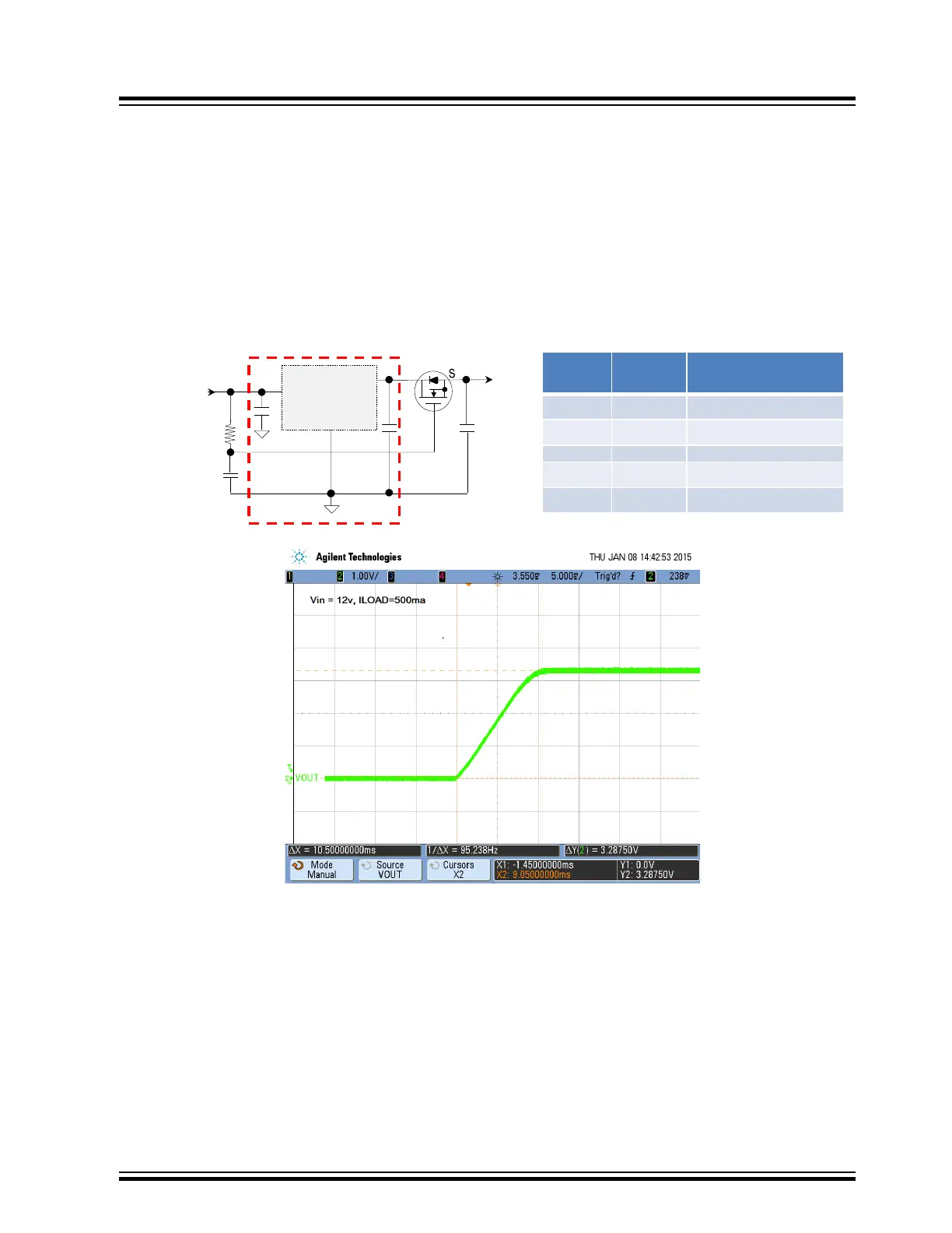
Figure 7-2. VDD Soft Start Circuit to Control VDD Ramp Rate
VIN RT =
Soft Start
VDD Ramp Time
5v 10k
~15±2ms
6v 14.3k ~18±2ms
9v 33.2k
~18±2ms
12v 49.9k ~18±2ms
16v 60.2k ~15±2ms
VOUT
Regulator
VIN (Max)
spec ≤ 18v
RT
1uf
25v
DMN2075U-7
(Up to 20v & 3.5A)
D
G
Users
Regulator
Circuit
Return to Checklist
7.2 Power Bypassing
Problem 2: Intermittent start-up, wake from low-power modes or analog repeatability issues.
Note
: Improper bypassing can affect the MCU during peak current demand periods during start-up, exit from low-
power modes to Active mode, and clock switching between low-frequency operation to a higher clock operating
frequency. It can also have an effect on timing jitter and pronounced analog peripheral performance impacts.
• All capacitors ceramic w/ESR ≤ 1 Ohm ideally.
• All caps located on same side of the PCB as the MCU, except with packages, such as BGA where interior
package pins are not accessible.
MCU Start-up Problems
© 2022 Microchip T
echnology Inc.
and its subsidiaries
Manual
DS70005439B-page 13