8. Unexpected Resets
Important: In the PIC32MX/PIC32MM/PIC32MZ/PIC32MK family of devices, if the user
’s code attempts
to modify at RUN time any configuration registers values in Flash, it can cause either a reset due to a
configuration register mismatch and a lock up. Refer to the RCON and RNMICON register for the cause of
the reset. Do not attempt any run time configuration register modifications.
8.1 PIC32MX/PIC32MM POR/BOR
Problem 12: Sometimes a reset happens on a wake from sleep, or during a clock switch.
•
On the PIC32MX/PIC32MM family of devices, on a wake from a sleep event, during a clock switch from a
relatively low frequency to full speed operation, when using IESO = 1, or two speed start-up, the instantaneous
current surge puts a strain on the internal LDO which has a finite response time to sudden current demand
changes. If the external VCAP bypass capacitor for the internal LDO is not at least 10 µF or better and has a
capacitor ESR < 1-3 Ohms, a POR or BOR can occur. The 10 µF VCAP is required to stabilize the internal LDO
during fast transient currents. A ceramic or solid tantalum cap is recommended. The lower the ESR the faster
the response to instantaneous current changes, and therefore, less internal LDO noise and voltage fluctuations.
8.2 PIC32MZ/PIC32MK/PIC32C POR/BOR
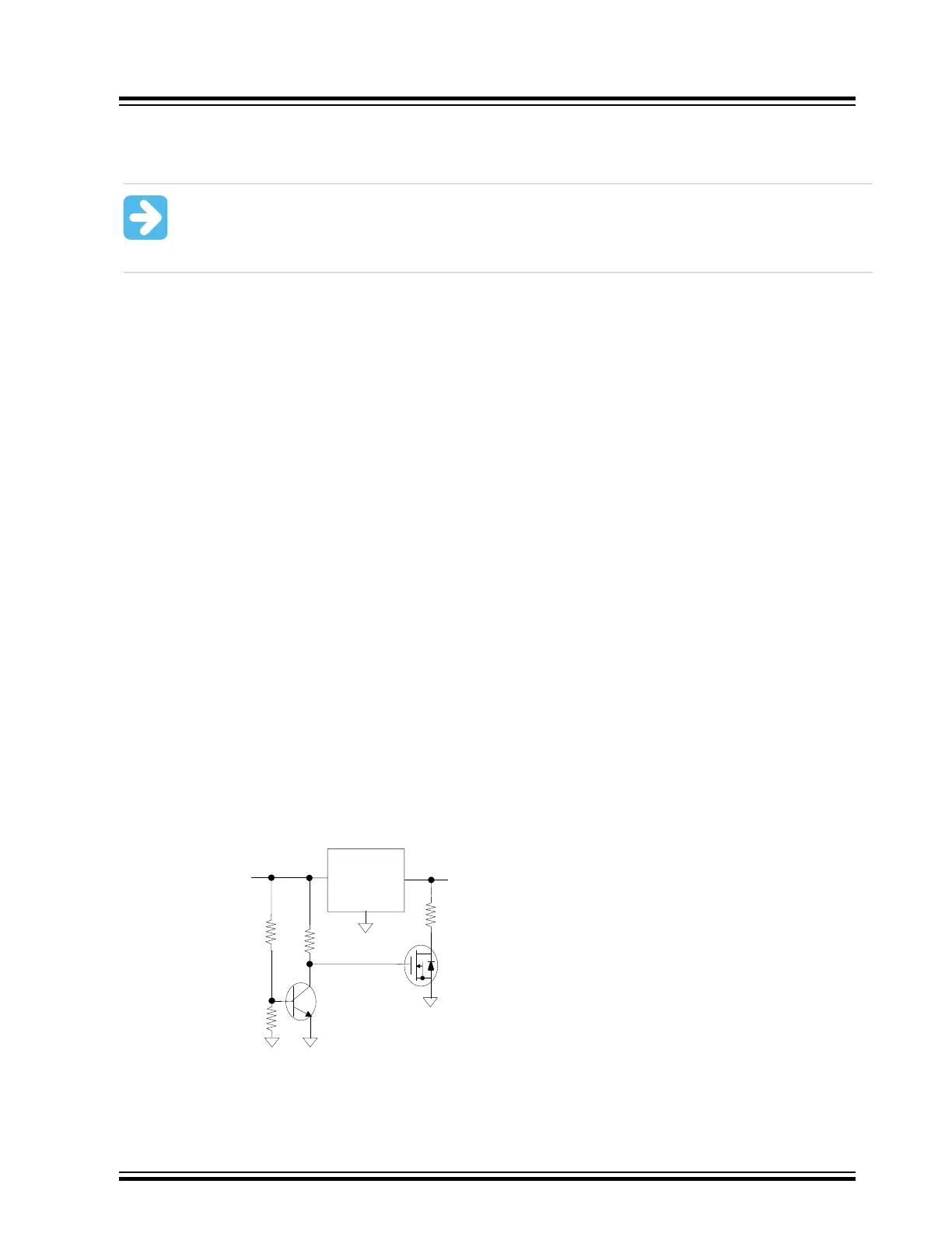
Problem 13: A lock-up sometimes occurs during a power anomaly or when power cycling the application.
On the PIC32MZ/PIC32MK and some PIC32C families, the “VPOR” data sheet spec is listed as:
•
VPOR = VSS+0.3v(max). Which means that to guarantee a proper Power-on Reset (POR) the VDD must fall
below the POR threshold. In situations where there are transient power anomalies or rapid power cycling of
the system, VDD may not always fall low enough or fast enough between the time the power loss began and
power levels being restored to normal. How fast the system VDD decays is a function of the amount of BULK
capacitance on the VDD power bus and the active load seen by the regulator. The circuit in the following figure
addresses the issue by rapidly pulling the VDD low when the regulator input voltage drops below the regulator’s
drop out voltage to force the VDD < 0.3v, and releases the VDD when input power levels return to ~90% of
normal.
Figure 8-1. PIC32MZ/PIC32MK VDD Crowbar Circuit
VIN VOUT
GND
10k
V
DD
V
IN
Transistor T1
BCW32LT1G
30Ω
VREG1
VDD CROWBAR CIRCUIT
G
S
D
RU1J002YNTCL
R1=10K
VBE(min) = Trans T1 VBE(min) spec
V
TRIP
= (V
DD
– (VREG1_V
DROPOUT
(min)+0.15))
R2 = (VBE(min) * 10k) / (V
TRIP
-VBE
(min)
)
NOTE: Round R2 down to 1 decimal point
R2
Unexpected Resets
© 2022 Microchip T
echnology Inc.
and its subsidiaries
Manual
DS70005439B-page 23