17.3 PCB Signal Integrity Concerns
1. Provide resistor terminations for all high-speed switching signals and clock lines >15 MHz on the PCB. Locate
these terminations on the driver side of the trace. The exception is high speed silicon impedance controlled
dif
ferential signal,s such as USB that do not require resistor termination because the drivers themselves have
guaranteed output impedance by specification.
For bi-directional signals, place a series resistor at the output of any output driver on the bus.
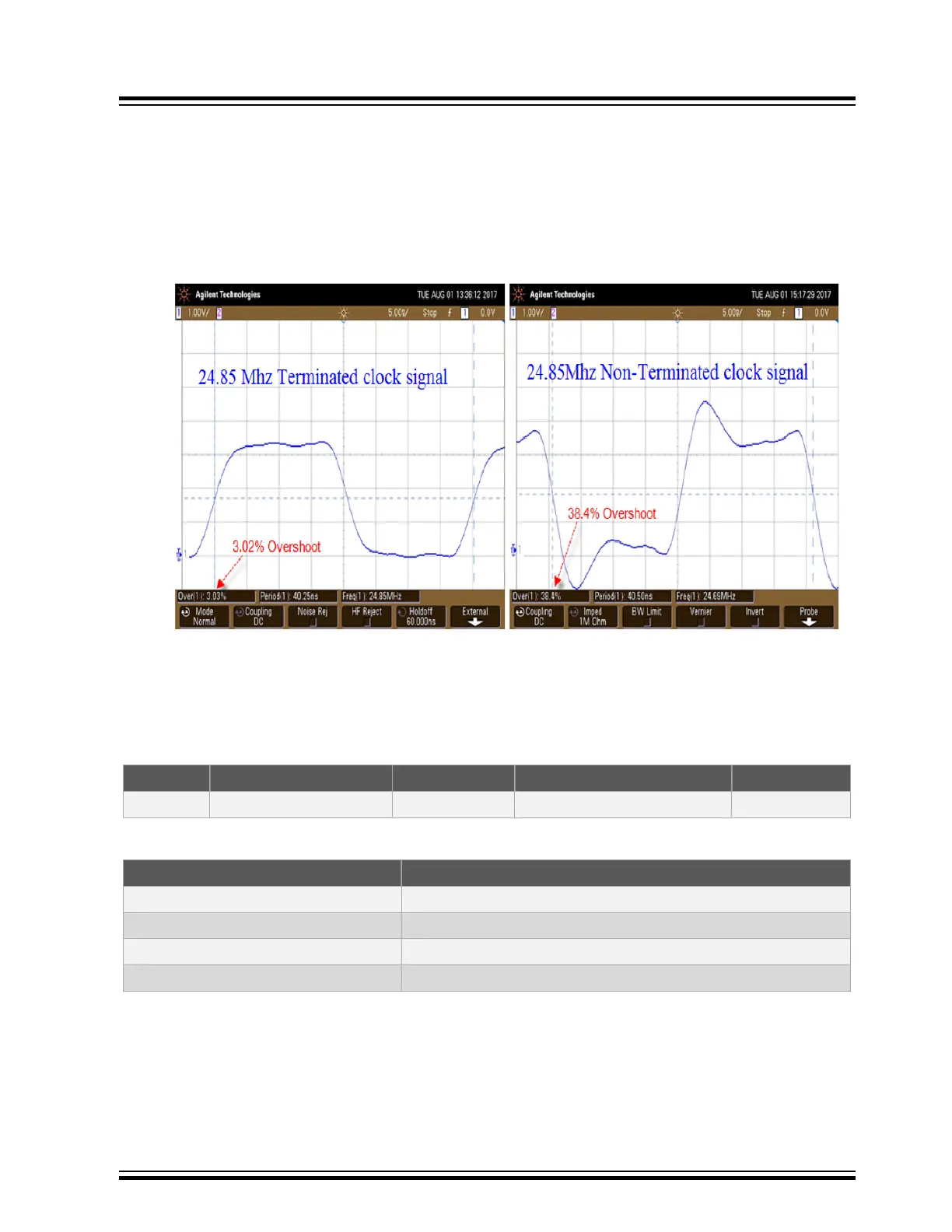
Figure 17-6. High Speed Signal Termination Scope Plot Illustration
There are two methods to determine the required termination resistor values.
Step 1: Calculate the PCB line impedance by entering the PCB trace information into an impedance
calculator:
https://www
.eeweb.com/tools/microstrip-impedance = Trace Impedance
Table 17-1. PCB Trace Impedance Calculation Example
Trace Width PCB Height between layers Trace Thickness PCB Substrate Dielectric FR4 Bd Trace Impedance
0.175mm 113µm 1.41 mils (1 oz Cu) 4 54.6 Ohms
Table 17-2. Typical Trace Thicknesses Based on Copper Weight
Cu weight Thickness in Mils
1 oz 1.4 mils
2 oz 2.8 mils
3 oz 4.2 mils
4 oz 5.6 mils
Step 2: Once the trace impedance is calculated by entering the PCB trace information then:
Method 1 of 2: (Ball Park method)
PCB signal series termination resistor(s) value = {[(VDD-VOH(min)) / IOH(max)] - T
race Impedance}
= {[(3.3-2.4) /10 ma] – 54.6 Ohms}
Comprehensive PCB Layout Guidelines and Recommenda...
© 2022 Microchip T
echnology Inc.
and its subsidiaries
Manual
DS70005439B-page 70