2. 6-Layer PCB Example:
–
Layer 1 component + signal side (short traces)
– Layer 2 ground plane
– Layer 3 signal
– Layer 4 signal
– Layer 5 power plane
– Layer 6 signal
Note: Layer 1 on either 4-layer or 6-layer PCB’s is considered the prime layer for critical routes and
components because of the solid digital ground plane directly beneath it and Layer 1 also requires no vias to
connect components located on Layer 1.
3. All PCB traces (especially high-speed and critical signal traces) must be routed on Layer 1 next to the solid,
contiguous ground plane layer. These traces must have a continuous reference plane for their entire length of
travel. This will help ensure optimum signal integrity and EMC performance.
4. The implementation of an Ethernet chassis ground plane separate from the digital ground plane is required.
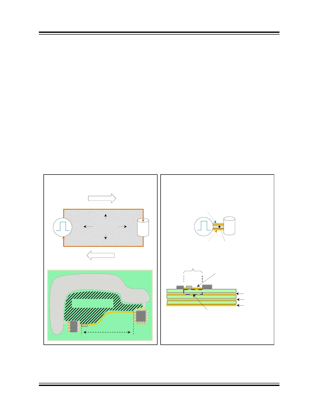
5. Avoid creating current loops in the PCB design and the system design. In order to facilitate routing and
minimize signal cross talk issues, adjacent layers in a multi-layer design should be routed orthogonal. Current
loops create excellent antennas and make the circuit very susceptible to picking up noise and radiated EMI.
The larger the current loop, the bigger the antenna, and the more noise it attracts. Poor PCB designs that
unintentionally create current ground loops are most common on 2-layer PCB designs. For high speed signals
these are one of the biggest issues leading to data corruption.
Figure 17-5. Current Loops in the PCB Design Diagram
Frequency
Current Loop
AREA
Load
current
current
<< G
ND RETURN
SIGNAL SOURCE >>
Frequency
Load
CIRCUIT_A
(Two Layer PCB Example)
CIRCUIT_B
(Four Layer PCB Example)
Continuous Ground
Plane Layer
Signal Trace
Current Loop
AREA
(PCB Layer Thickness)
GND
HS Signal
Current Loop AREA
Length X
HS Signal
GND Plane L2
PWR Plane L3
Signal L4
Signal Layer 1
Length ¼ X
Current Loop AREA
4-Layer PCB Edge View
2-Layer PCB Top View
Comprehensive PCB Layout Guidelines and Recommenda...
© 2022 Microchip T
echnology Inc.
and its subsidiaries
Manual
DS70005439B-page 69