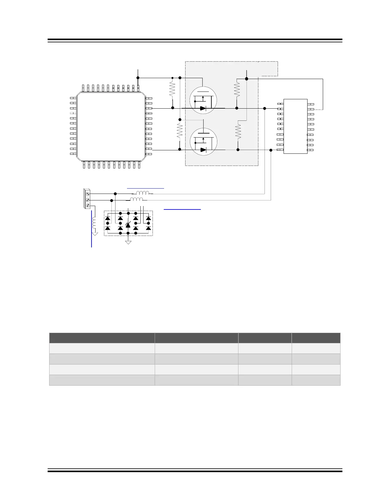
Figure 14-1. I
2
C Protection Design Diagram
VDD
1
= 2.6-3.6v
DMN65D8L-7
2.2k
DMN65D8L-7
2.2k
3.3k
3.3k
MPU
(2.6-3.6v)
SCL
SDA
1
D5V0P4UR6SO
2
3
4
5
6
3
2
1
SCL
GND
SDA
MI0805J102R-10
MI0805J102R-10
IC
SCL
SDA
SD
G
SD
G
OPTIONAL I2C
Level Shifter
MI0805J102R-10
1kΩ @ 100MHz, DCR=0.15Ω, 1A
VDD2 ≥ VDD
1
5v
14.1 Key I
2
C Protection Design Points
There is an optional level shifter to interface 3.3V nominal logic to a 5V and higher nominal logic. When a low
voltage I
2
C node signal level goes low
, the FET is turned on pulling the higher voltage I
2
C bus low also. When the
high-voltage node side goes low, it forward biases the FET internal diode pulling the low-voltage node side low minus
the diode drop. When both side are high the FET is off, and the FET internal diode is reverse biased.
• ESD protection on ground, SDA, and SCL
Table 14-1. Example I2C Level Shifter Logic Truth Table
3.3v Low Voltage side I
2
C Node (MCU) 5v High voltage side I
2
C node 3.3v I
2
C node side 5v I
2
C node side
0 0 0v 0v
1 0 0.3v 0v
0 1 0v 0v
1 1 3.3v 5v
Return to Checklist
I2C
© 2022 Microchip T
echnology Inc.
and its subsidiaries
Manual
DS70005439B-page 59