Note: Not all connectors like audio metal input/output jack cases are isolated. They are in fact the signal
ground. In situations like that they must not be mounted to an isolated AC chassis ground, but instead to the
digital/analog ground as appropriate using a ferrite bead (see audio circuit design protection example). The
user must determine for the external peripheral connector in use if it has an isolated or non-isolated case to
signal ground or not. For isolated connectors, connect only the connector case to the AC chassis ground,
otherwise connect to signal ground through an appropriate ferrite bead.
On the second example where there is no AC chassis ground (i.e. earth ground) available, the best strategy is
to still have an isolation barrier and join the inner and other planes at the lowest impedance point in the circuit
relative to the power source at the power inlet and regulator (otherwise called power ground). This will divert
high energy discharges on the external connectors and shields around sensitive digital and analog circuitry to
be dissipated through the power source and coupled back into the AC mains.
14.
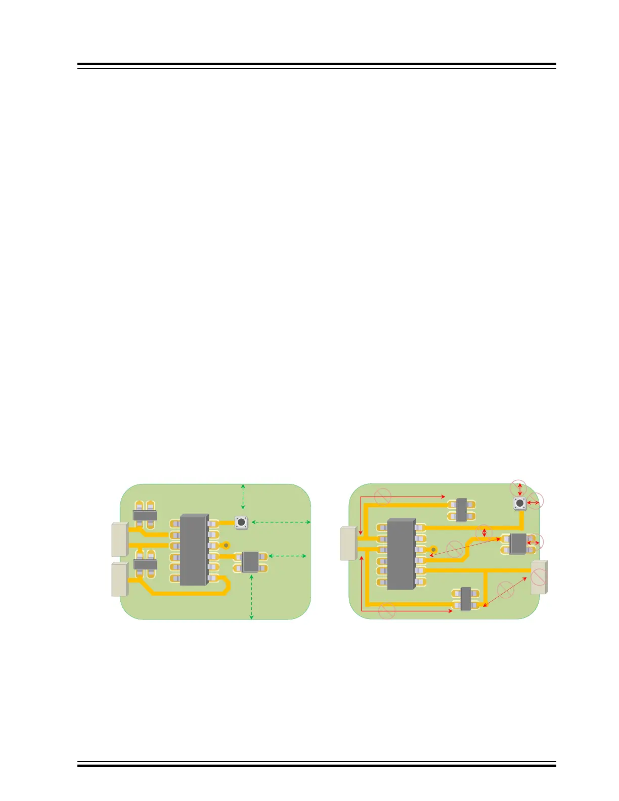
No high-speed circuitry should be located between I/O connectors. Even if two connectors are on the same
edge of the board, high-speed circuitry located between them can induce enough common-mode voltage to
drive one connector relative to the other resulting in significant radiated emissions.
15. Critical signal or clock traces when possible should be buried between power/ground planes. Routing a trace
on a layer between two solid planes does an excellent job of containing the fields from these traces and
prevents unwanted coupling.
16. Select active digital components that have maximum acceptable off-chip transition times. If the transition times
of a digital waveform are faster than they need to be, the power in the upper harmonics can be much higher
than necessary. If the transition times of the logic employed are faster than they need to be, they can usually
be slowed using series resistors or ferrites.
17. All off-board communication from a single device should be routed through the same connector. Many
components (especially large VLSI devices) generate a significant amount of common-mode noise between
different I/O pins. If one of these devices is connected to more than one connector, this common-mode noise
will potentially drive a good antenna (The device will also be more susceptible to radiated noise brought in on
this antenna).
18. Locate Transient Voltage Suppressors (TVS) as close to external signal connectors as possible with the TVS
ground connecting directly to the ground plane. Avoid ground trace connections.
19. High-speed or susceptible analog or digital traces must be routed at least 2X from the board edge, where ‘X’ is
the distance between the trace and its return current path. The electric and magnetic field lines associated with
traces very near the edge of a board are less well contained. Crosstalk and coupling to and from antennas
tend to be greater from these traces and makes them more susceptible to ESD, EMI, and EFT events.
Figure 17-4. Printed Circuit Board Layout Examples
P
r
o
t
e
c
t
e
d
D
e
v
i
c
e
C
O
N
N
TVS
Bad ESD/ EMI / TVS PCB Layout
TVS
OSC
R
Reset PB
C
O
N
N
TVS
TVS
Good ESD/EMI/TVS PCB Layout
OSC
R
Reset PB
C
O
N
N
C
O
N
N
P
r
o
t
e
c
t
e
d
D
e
v
i
c
e
20. Differential signal trace pairs must be routed together and maintain the same distance from any solid planes.
Dif
ferential signals are less susceptible to noise and less likely to generate radiated emissions if they are
balanced (i.e., If they have the same length and maintain the same impedance relative to other conductors).
21. All power (for example, voltage) planes that are referenced to the same power return (for example, ground)
plane, must be routed on the same layer. For example, if a board employs three voltages: 3.3 volts, 3.3 volts
analog, and 1.8 volts, then it is generally desirable to minimize the high-frequency coupling between these
planes. Putting the voltage planes on the same layer will ensure that there is no overlap. It will also help to
Comprehensive PCB Layout Guidelines and Recommenda...
© 2022 Microchip T
echnology Inc.
and its subsidiaries
Manual
DS70005439B-page 67