© Microhard Systems Inc. CONFIDENTIAL 27
IP9xx Series
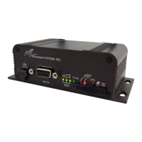
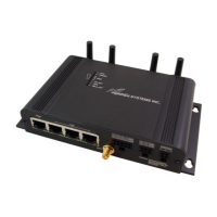
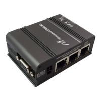
3.0 Hardware Features
Pin Name No. Description In/
Out
Vcc 1,3 Positive supply voltage for the module (9-30
VDC)
I
VRF 2 Voltage Output (4.5VDC) O
!CONFIG 4 Active low input signal to put the module into
FLASH FILE SYSTEM RECOVERY mode.
I
GND 5,7 Ground reference for logic, radio and I/O pins.
+3V3 FPGA 6 Voltage Output ON during sleep mode.
(3.3VDC)
O
+3V3 8 Voltage Output OFF during sleep mode.
(3.3VDC)
O
NC 9-18 *Reserved for factory use.*
TXD0 19 Data Port. Transmit Data. Logic Level Output
from the modem.
O
NC 20-21 *Reserved for future use.*
CTS1 22 Diagnostics Port. Clear To Send. Active low
output.
O
CTS0 23 Data Port. Clear To Send. Active low output. O
RTS1 24 Diagnostics Port. Request To Send. Active low
input.
I
RTS0 25 Data Port. Request To Send. Active low input. I
TXD1 26 Diagnostics Port. Transmit Data. Logic level
output from modem.
O
RXD1 27 Diagnostics Port. Receive Data. Logic level
input into the modem.
I
DCD0 28 Data Port. Data Carrier Detect. Active low
output.
O
DTR0 29 Data Port. Data Terminal Ready. Active low
input.
I
DSR0 30 Data Port. Data Set Ready. Active low output. O
GND 31-32 Ground reference for logic, radio, and I/O pins
Table 3E: SIP921 Pin-Out Description