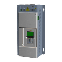
SPDM CONTROL BOX SUMMARY
NIDEC ASI S.P.A. – SPDM CONTROL BOX USER MANUAL
IMSPDCB2EN I
SUMMARY
Manufacturer .............................................................................................................................................................................................................1
Manufacturer address................................................................................................................................................................................................1
Warranty and limitation of liability..............................................................................................................................................................................1
Introductions and warnings for the purchaser ...........................................................................................................................................................2
User Manual ..............................................................................................................................................................................................................3
Safety rules contained in the manual ........................................................................................................................................................................4
Symbols used............................................................................................................................................................................................................5
Safety symbols ..........................................................................................................................................................................................................6
Terms and acronyms.................................................................................................................................................................................................8
Warranty ....................................................................................................................................................................................................................9
SPDM CONTROl BOX management ......................................................................................................................................................................10
1 TECHNICAL DATA....................................................................................................................................................................................11
1.1 Identification........................................................................................................................................................................................11
1.2 Plate....................................................................................................................................................................................................11
1.3 Technical data ....................................................................................................................................................................................11
1.4 Admissible environmental conditions .................................................................................................................................................12
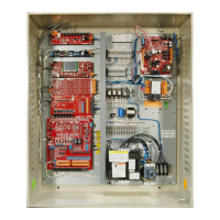
2 Composition of the CONTROL box ...........................................................................................................................................................15
2.1 TYPICAL USE ....................................................................................................................................................................................15
2.2 INTERNAL CONNECTIONS ..............................................................................................................................................................15
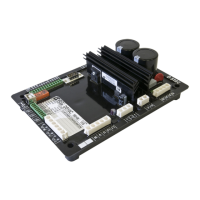
2.3 Control board “SYSTEM2” (cod. 1000261943) ..................................................................................................................................18
2.4 Interface board “GPSIA” (cod. 1000253095)......................................................................................................................................18
2.4.1 GPSIA Layout ..............................................................................................................................................................................19
2.4.2 Connectors ..................................................................................................................................................................................19
2.4.3 Jumpers .......................................................................................................................................................................................19
2.5 Fiber optics board “GIFOA” (cod. 1000253641).................................................................................................................................20
2.5.1 GIFOA Layout..............................................................................................................................................................................20
2.5.2 Connectors ..................................................................................................................................................................................21
2.5.3 Jumpers .......................................................................................................................................................................................21
2.6 GPTRA board (cod. 1000253094)......................................................................................................................................................21
2.6.1 GPTRA Layout.............................................................................................................................................................................22
2.6.2 Jumper settings ...........................................................................................................................................................................22
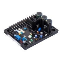
2.7 Power board “BPR50” (also called “P” board) (cod. ELC452441)......................................................................................................22
2.7.1 Board P customizing..................................................................................................................................................................22
2.7.2 CT load resistors.........................................................................................................................................................................23
2.7.3 P Board terminals and test points.............................................................................................................................................24
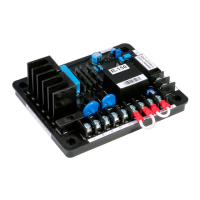
2.8 Power supply board “GAAPA” (cod. 1000080550).............................................................................................................................25
2.9 Switched Mode Power Supply (cod. 8000002668) ............................................................................................................................26
2.10 Keypad (cod. 8000001597) ................................................................................................................................................................26
2.11 Encoder Interface “SYSENC”.............................................................................................................................................................26
2.11.1 General data ................................................................................................................................................................................26
2.11.2 Connection and jumpers presetting with System board ..............................................................................................................28
2.11.3 J2, connector for power supply of module SYSENC...................................................................................................................28
2.11.4 J3, encoder inputs removable terminal blocks ............................................................................................................................28
3 “SYSTEM2” BOARD..................................................................................................................................................................................31
3.1 Jumpers, switches and buttons ..........................................................................................................................................................32
3.1.1 Jumpers .......................................................................................................................................................................................32
3.1.2 Buttons.........................................................................................................................................................................................36
3.1.3 Switches.......................................................................................................................................................................................36
3.2 Connectors .........................................................................................................................................................................................37
3.2.1 Description of the connectors ......................................................................................................................................................37
3.2.2 J16, connector Modbus ...............................................................................................................................................................38
3.2.3 J17, connector CANBus ..............................................................................................................................................................38
3.2.4 J18, auxiliary Opto-isolated digital outputs..................................................................................................................................39
3.2.5 J19, connector Profibus DP.........................................................................................................................................................40
3.2.6 J23, extractable terminal blocks ..................................................................................................................................................40
3.3 LEDs...................................................................................................................................................................................................42
3.3.1 Description of the onboard LEDs.................................................................................................................................................42
3.3.2 DL1DL4, DL6, general purpose led ............................................................................................................................................43
3.3.3 DL5, monitor of power supply 6,5V .............................................................................................................................................43
3.3.4 DL7, monitor for signal PROTHW_B ...........................................................................................................................................43
3.3.5 DL8, monitor for signal ABIL_B ...................................................................................................................................................43
3.3.6 DL9, monitor for signal DRIVEOK_B...........................................................................................................................................43
3.3.7 DL10, monitor of the intervention of Watch-Dog between processors........................................................................................43
3.3.8 DL11, monitor of signal PROTHW_A ..........................................................................................................................................43
3.3.9 DL12, monitor of signal ABIL_A...................................................................................................................................................43
3.3.10 DL13, monitor of signal DRIVEOK_A ..........................................................................................................................................44