Clock calculator design
MPC5777C Clock Calculator Guide, Rev. 1, 12/2018
14 NXP Semiconductors
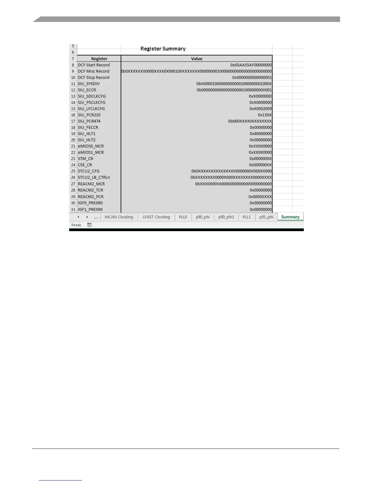
Figure 17. Register summary table
The register values are displayed in either hexadecimal or binary format, where a “0x” prefix represents
hexadecimal and “0b” denotes binary. A capital “X” represents a “don’t care” bit/half-byte. These bits
do not affect the clock frequency, so users can set these values to whatever suits their purposes. Users
can best utilize Summary by setting the configuration they want in the clock calculator and then copying
the resulting register value into code. For example, taking from the figure above, the register
SIU_LFCLKCFG should be set to 0xX0002009. Assuming the instances of “X” are “0”, the resulting
S32DS C code would be: “SIU.LFCLKCFG.R = 0x00002009;”.
Summary also includes an overview of the clock domain frequencies. Since this tool consists of multiple
interdependent spreadsheets, it might be cumbersome for users to weave through them all to find a clock
domain. This table provides a place where all of them can be found. The table is organized by module,
followed by the clock type (i.e. BIU clock, peripheral clock, protocol clock, etc.), and finally the
frequency, as currently configured. Below is a screenshot of clock summary table.

 Loading...


