Table 11. POR configuration through switches (continued)
Switch Signal name Pin name Signal meaning Setting
SW3[2:3] cfg_eng_use[1:2] Reserved Reserved -
SW3[4] BOOT_FLASH_S
EL
- Boot flash selection
SW3[4] = 0 for NOR boot
SW3[4] = 1 for NAND boot
See note
1
SW3[5:7] CFG_VBANK[0:2] - NOR flash bank select
000: bank0
100: bank4
See note
2
SW3[8] TEST_SEL_N TEST_SEL_B - 1:T2080
1. For SW3[4]: BOOT_FLASH_SEL, it can act as boot flash selection, when BOOT_FLASH_SEL=1, NOR flash is boot flash or
NAND flash is boot flash.
2. SW3[5:7] can be used to change the staring address for the memory banks. The NOR flash memory is divided into eight
memory banks with 16 MB size each. Eight different U-Boot images can be programmed into each memory bank. When NOR
flash is selected as boot flash (CS0 is connected to NOR flash by setting SW3[4] to ON, RCW[0:8] is set to 0_0111_xxxx using
SW1[1:8] and SW2[1]), different U-Boot image can be selected to boot up the board, by setting SW3[5:7].
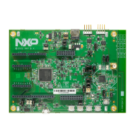
NXP Semiconductors
Architecture
QorIQ T2080 Reference Design Board (T2080RDB-PC) User Guide, Rev. 1, 08/2021
User Guide 29 / 44
 Loading...