Appendices
A-46
CJ2 CPU Unit Hardware User’s Manual
*1 The ON response time will be 20 µs maximum and OFF response time will be 400 µs maximum even if the response
times are set to 0 ms due to internal element delays.
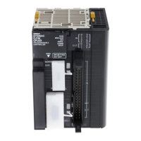
Terminal Connections
CN1 (OUT) CN2 (IN)
• When wiring, pay careful attention to the polarity
of the external power supply. The load may oper-
ate incorrectly if polarity is reversed.
• Be sure to wire both pins A9 and B9 (COM0
(0 V)) of CN1.
• Be sure to wire both pins A10 and B10 (+V) of
CN1.
• When wiring, pay careful attention to the polarity of
the external power supply. The load may operate
incorrectly if polarity is reversed.
• Be sure to wire both pins A9 and B9 (COM1) of
CN2, and set the same polarity for both pins.
A1
A2
A3
A4
A5
A6
A7
A8
OUT0
OUT1
OUT2
OUT3
OUT4
OUT5
OUT6
OUT7
A9
A10
A11
A12
NC
NC
COM0 (0V)
+V
B1
B2
B3
B4
B5
B6
B7
B8
B9
OUT9
OUT10
OUT11
OUT12
OUT13
OUT14
OUT15
OUT8
B10
B11
B12
L
L
L
L
L
L
L
L
L
L
L
L
L
L
L
L
NC
COM0 (0V)
+V
NC
12 to
24
VDC
Wd m
Wd m
Signal
name
Signal
name
Connec-
tor pin
Allocated
CIO word
Allocated
CIO word
B12
B11
B10
B9
B8
B7
B6
B5
IN15
IN14
IN13
IN12
IN11
IN10
IN9
IN8
B4
B3
B2
B1
A12
A11
A10
A9
A8
A7
A6
A5
A4
IN6
IN5
IN4
IN3
IN2
IN1
IN0
IN7
A3
A2
A1
NC
COM1
NC
NC
NC
NC
COM1
NC
24 VDC
Wd m+1
Wd m+1
Signal
name
Signal
name
Connec-
tor pin
Allocated
CIO word
Allocated
CIO word