A-55
Appendices
CJ2 CPU Unit Hardware User’s Manual
A-1 Specifications of Basic I/O Units
App
A-1-2 Basic I/O Units
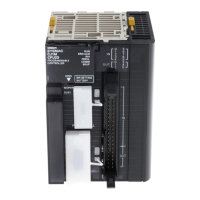
z CJ1W-MD563 TTL I/O Unit (32 Inputs/32 Outputs)
Name 32-point Input /32-point Output TTL I/O Unit with MIL Connectors
Model CJ1W-MD563
Output section (CN1) Input section (CN2)
Rated Voltage
5 VDC±10%
Rated Input Volt-
age
5 VDC±10%
Operating Load Voltage
Range
4.5 to 5.5 VDC
Input Impedance
1.1 kΩ
Maximum Load Current
35 mA/point, 560 mA/com-
mon, 1.12 A/Unit
Input Current
Approx. 3.5 mA (at 5 VDC)
Leakage Current 0.1 mA max. ON Voltage 3.0 VDC min.
Residual Voltage 0.4 V max. OFF Voltage 1.0 VDC max.
ON Response Time
0.2 ms max.
ON Response
Time
8.0 ms max. (Can be set to between 0 and 32 in the
PLC Setup.)
*1
OFF Response Time 0.3 ms max.
OFF Response
Time
8.0 ms max. (Can be set to between 0 and 32 in the
PLC Setup.)
*1
No. of Circuits
32 points (16 points/com-
mon, 2 circuits)
Fuse None No. of Circuits 32 points (16 points/common, 2 circuits)
External Power Supply
5 VDC±10%, 40 mA min.
(1.2 mA × No. of ON points)
Number of Simul-
taneously ON
Points
100% (16 points/common)
Insulation Resistance 20 MΩ between the external terminals and the GR terminal (at 100 VDC)
Dielectric Strength
1,000 VAC between the external terminals and the GR terminal for 1 minute at a leakage current of 10 mA
max.
Internal Current Consump-
tion
5 VDC 190 mA max.
Weight 110 g max.
Accessories None
Circuit Configuration
CN1 (OUT) CN2 (IN)
OUT0
+V
OUT15
COM0
OUT0
+V
OUT15
COM1
COM0
COM1
5.6 k
Ω
5.6 k
Ω
Output
indicator
Indicator
switch
Internal circuits
to
to
Wd m
Wd m+1
Allocated
CIO word
Signal
name
IN0
IN15
COM2
IN0
IN15
COM3
COM2
COM3
to
Indicator switch
Input indicator
Internal circuits
to
1.1 kΩ
2.2 k
Ω
1000 pF
1.1 kΩ
2.2 k
Ω
1000 pF
Wd m+2
Wd m+3
Allocated
CIO word
Signal
name