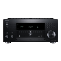
Do you have a question about the Onkyo TX-RZ800 and is the answer not in the manual?
High-level block diagram showing audio signal paths, digital processing, DACs, and MPU connections.
Block diagram illustrating the power supply units, transformers, relays, and voltage regulation for the AV receiver.
Schematic section detailing the final stage of the power amplifier for each channel, including transistors and output stages.
Schematic of the Analog Signal Processing (ASP) section, showing input selectors, volume control, and DACs.
Schematic section related to amplifier protection circuits, including thermal detection, voltage protection, and current detection.
Schematic detailing the speaker terminal connections, relays for channel selection, and protection circuits.
Schematic of the left channel amplifier voltage stage, showing input, bias, and output circuitry.
Schematic of the right channel amplifier voltage stage, showing input, bias, and output circuitry.
Schematic of the center channel amplifier voltage stage, showing input, bias, and output circuitry.
Schematic of the surround left (SL) channel amplifier voltage stage, showing input, bias, and output circuitry.
Schematic of the surround right (SR) channel amplifier voltage stage, showing input, bias, and output circuitry.
Schematic of the surround back left (SBL) channel amplifier voltage stage, showing input, bias, and output circuitry.
Schematic of the surround back right (SBR) channel amplifier voltage stage, showing input, bias, and output circuitry.
Schematic of the main 8-channel DAC, detailing digital audio inputs, clock signals, and analog outputs.
Schematic showing analog video inputs (Y/Pb/Pr, Y/C, CVBS) and outputs, including UP-conversion processing.
Diagram illustrating connections between different internal boards via connectors like P2101B, P2792, P2793, P4511B, P4591B.
Schematic showing the thermal sensor (LM61CIZ) connected to the amplifier circuitry and its associated components.
Schematic of the display control circuitry, including FL driver, key inputs, LED control, and microphone interface.
Schematic detailing key inputs, LED indicators, and standby/zone controls for the display unit.
Schematic for the microphone input on the display board, showing connections to the MICDET and MIC_IN pins.
Schematic illustrating the volume control interface, including connections for volume potentiometers and master volume settings.
Schematic for the headphone output, showing connections for HP_L, HP_R, HPDET, and GND_DG.
Schematic of the tuner section for DTR-50.7/60.7 and DHC-60.7 models, detailing RF, IF, and control signals.
Schematic of the display section, showing connections for various audio DACs and digital audio interfaces.
Schematic for the display section's headphone output board, showing headphone jack connections and related components.
Schematic of the power supply section for the display board, showing voltage regulators and power distribution.
Schematic of the power supply section for the amplifier boards, detailing relays, fuses, and voltage outputs.
Schematic of the Power Supply (PS) section for DHC-60.7, showing SMPS, transformers, and safety precautions.
Schematic of the Microprocessor Unit (MPU) section, detailing its connections to EEPROM, various interfaces, and other ICs.
Schematic of the Video Processing Unit (VMPU) section, showing connections to HDMI, HD-BaseT, and various interface signals.
Schematic of the Video Signal Processing (VSP) section, detailing connections for HDMI RX, TMDS signals, and CEC communication.
Schematic of the HDMI Receiver 1 (RX1) section, showing TMDS signal paths, DDC, CEC, and HPD control lines.
Schematic of the HDMI Receiver 2 (RX2) section, including SD video decoder and connections to other digital interfaces.
Schematic of the power supply for the network and USB interfaces, detailing voltage regulators and power sequencing.
Schematic of the ARM processor and Zone DAC connections, showing digital audio interfaces and clock signals.
Schematic illustrating the connections for the ARM processor's memory interface, including SDRAM, NAND, and JTAG signals.
Schematic of the Digital Signal Processor (DSP) section, showing connections for SDRAM, serial interfaces, and clock signals.
Schematic of the main power supply circuits, including various voltage regulators and power control logic.
Schematic detailing the balance output stages for main channels, including operational amplifiers and output relays.
Schematic for balance input/output connections, showing XLR inputs, DAC outputs, and associated circuitry.
Schematic of the balance output section for DHC-60.7, illustrating speaker relays and output driver stages.
Schematic showing Analog Signal Processing (ASP) and Video connections between boards, detailing connector pinouts.
Schematic of the front HDMI input section, showing TMDS signal routing, DDC, CEC, and HP detection for DTR models.
 Loading...