EasyManua.ls Logo

Onkyo TX-SR674E Service Manual

Onkyo TX-SR674E
127 pages
To Next Page IconTo Next Page
Page #1 background imageLoading...
Page #1 background image
MD-2000
TX-SR674/674E/8460
SERVICE MANUAL
Ref. No. 3949
102006
AV RECEIVER
MODEL
TX-SR674
MODEL TX-SR674E
MODEL TX-SR8467
TX-SR674 Black, Golden and Silver models
230-240V AC, 50Hz
120V/220-24 0V AC, 50/60Hz
220-230V AC, 50/60Hz
B MPA, S MPA
B MWT, B MWO, G MWT, G MWO
G MGR, G MGQ, G MGK
TX-SR674E Black and Silver models
230-240V AC, 50Hz
B MPP, B MPB, S MPP, S MPB
TX-SR8467
Golden model
220-230V AC, 50/60Hz
G MGR
RC-651M
SAFETY-RELATED COMPONENT
WARNING!!
COMPONENTS IDENTIFIED BY MARK ON THE
SCHEMATIC DIAGRAM AND IN THE PARTS LIST ARE
CRITICAL FOR RISK OF FIRE AND ELECTRIC SHOCK.
REPLACE THESE COMPONENTS WITH ONKYO
PARTS WHOSE PART NUMBERS APPEAR AS SHOWN
IN THIS MANUAL.
MAKE LEAKAGE-CURRENT OR RESISTANCE
MEASUREMENTS TO DETERMINE THAT EXPOSED
PARTS ARE ACCEPTABLY INSULATED FROM THE
SUPPLY CIRCUIT BEFORE RETURNING THE
APPLIANCE TO THE CUSTOMER.
MUTING
PREVIOUS
MENU
GUIDE
TOP MENU
SETUPRETURN
PLAYLIST/CAT PLAYLIST/CAT
RANDOM
SUBTITLE
PLAY MODE
AUDIO REPEAT
RC
-
651M
--
/
---
TAPE
MD/CDR
HDD
CABLE
ON/STANDBY
DIMMER
ENT
D TUN
SLEEP
10 11 12
INPUT SELECTOR
HDDDVDVCR
REMOTE MODE
ZONE2
V1
V4
V2 V3
CDTAPE TUNER
DVD
MULTI CH
LISTENING MODE
TV
DISPLAY
TEST TONE
CH SEL
SURROUND
STEREO
CINE FLTR
LEVEL
+
LEVEL
-
L NIGHT
VOL
VOL
SAT
VCR
TV
DVD
RECEIVER
CD
INPUT
+
10
0
CLR
123
456
789
ENTER
CH
DISC
ALBUM
TX-SR674
B MDD, B MDC, S MDC
120V AC, 60Hz
Question and Answer IconNeed help?

Do you have a question about the Onkyo TX-SR674E and is the answer not in the manual?
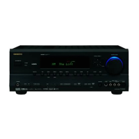
Onkyo TX-SR674E Specifications

General IconGeneral
Audio Channels7.1
Power Output100 W
Total Harmonic Distortion0.08%
HDMI Inputs3
HDMI Outputs1
Component Video Inputs3
Component Video Outputs1
Digital Audio Inputs (Optical)2
Digital Audio Inputs (Coaxial)2
Input Sensitivity200 mV
Signal-to-Noise Ratio (SNR)106 dB
Signal-to-Noise Ratio106 dB
Dimensions (W x H x D)435 x 174 x 377 mm
Frequency Response (extended)10 Hz - 100 kHz
Audio Inputs/Outputs (Digital Optical)2
Audio Inputs/Outputs (Digital Coaxial)2
Surround Sound ModesDolby Digital, DTS
Video Inputs/Outputs (Composite)4 inputs / 1 output

Summary

AV Receiver Models and Power Requirements

TX-SR674 Black, Golden, Silver Models

Power requirements for TX-SR674 Black, Golden, and Silver models.

TX-SR674E Black, Silver Models

Power requirements for TX-SR674E Black and Silver models.

TX-SR8467 Golden Model

Power requirements for TX-SR8467 Golden model.

Safety-Related Component Warnings

Critical Component Handling and Safety Checks

Procedures for replacing critical components and ensuring safety.

Service Procedures

Fuse Replacement

Guidelines and part numbers for fuse replacement.

Operation Check-1: Speaker Protect-1 (DC Voltage Detection)

Operation Check-2: Speaker Protect-2 (Current Detection)

Check Procedure

Detailed steps for current detection speaker protection test.

Operation Check-3: Power Supply Control

Sensor Check Procedure

Steps to check output and thermal sensors.

Operation Check-4(1/2): DSP Debug Mode

Operation Check-4(2/2): DSP Debug Mode Analysis

Troubleshooting DSP Issues via Debug Mode

Table correlating symptoms, causes, and checks for DSP problems.

Block Diagram-1: Audio Section Overview

Audio Section Block Diagram

Overall block diagram of the audio signal path.

Block Diagram-1: Audio Section Overview (Continued)

Audio Section Block Diagram (Continued)

Continuation of the audio signal path block diagram.

Block Diagram-2: Video Section-1 Overview

Video Section-1 Block Diagram

Block diagram of video input and processing.

Block Diagram-2: Video Section-1 Overview (Continued)

Video Section-1 Block Diagram (Continued)

Continuation of video input/processing block diagram.

Block Diagram-3: Video Section-2 Overview

Video Section-2 Block Diagram

Block diagram of HDMI input and processing.

Block Diagram-3: Video Section-2 Overview (Continued)

Video Section-2 Block Diagram (Continued)

Continuation of HDMI input/processing block diagram.

Schematic Diagram-1(SD-1): Audio Section

Audio Section Schematic Part 1

Detailed schematic of the audio section, part 1.

Schematic Diagram-1(SD-1): Audio Section (Continued)

Audio Section Schematic Part 1 (Continued)

Continuation of audio section schematic, part 1.

Schematic Diagram-2(SD-2): Power Amp Section-1

Power Amp Section-1 Schematic Part 1

Schematic of the power amplifier section, part 1.

Schematic Diagram-2(SD-2): Power Amp Section-1 (Continued)

Power Amp Section-1 Schematic Part 1 (Continued)

Continuation of power amplifier schematic, part 1.

Schematic Diagram-3(SD-3): Power Amp Section-2

Power Amp Section-2 Schematic Part 2

Schematic of the power amplifier section, part 2.

Schematic Diagram-4(SD-4): Video Section

Video Section Schematic Part 1

Schematic of the video input/output section.

Schematic Diagram-4(SD-4): Video Section (Continued)

Video Section Schematic Part 1 (Continued)

Continuation of video input/output schematic.

Schematic Diagram-5(SD-5): Power Supply Section

Schematic Diagram-5(SD-5): Power Supply Section (Continued)

Schematic Diagram-6(SD-6): DSP Section

DSP Section Schematic Part 1

Schematic of the DSP section.

Schematic Diagram-6(SD-6): DSP Section (Continued)

DSP Section Schematic Part 1 (Continued)

Continuation of DSP section schematic.

Schematic Diagram-7(SD-7): XM Section

XM Section Schematic Part 1

Schematic of the XM section.

Schematic Diagram-7(SD-7): XM Section (Continued)

XM Section Schematic Part 1 (Continued)

Continuation of XM section schematic.

Schematic Diagram-8(SD-8): Display Section

Display Section Schematic

Schematic of the display section.

Schematic Diagram-9(SD-9): Power Supply Section

Power Supply Section Schematic Part 1

Schematic of the power supply section, part 1.

Schematic Diagram-9(SD-9): Power Supply Section (Continued)

Power Supply Section Schematic Part 1 (Continued)

Continuation of power supply schematic, part 1.

Schematic Diagram-10(SD-10): HDMI Section-1

HDMI Section-1 Schematic Part 1

Schematic of the HDMI section, part 1.

Schematic Diagram-10(SD-10): HDMI Section-1 (Continued)

HDMI Section-1 Schematic Part 1 (Continued)

Continuation of HDMI section schematic, part 1.

Schematic Diagram-11(SD-11): HDMI Section-2

HDMI Section-2 Schematic Part 1

Schematic of the HDMI section, part 2.

Schematic Diagram-11(SD-11): HDMI Section-2 (Continued)

HDMI Section-2 Schematic Part 1 (Continued)

Continuation of HDMI section schematic, part 2.

Schematic Diagram-12(SD-12): Digital Audio Waveforms

Digital Audio Waveform Analysis

Diagrams of digital audio signal waveforms and properties.

IC Block Diagram and Terminal Descriptions -1

Q7003: M66005 (FL Tube Driver) - Block Diagram

Block diagram of the FL Tube Driver IC.

Q7003: M66005 (FL Tube Driver) - Terminal Description

Terminal descriptions for the FL Tube Driver IC.

IC Block Diagrams and Terminal Descriptions -2

Q2001: F2602E (XM Digital Transceiver) - Block Diagram

Block diagram of the XM Digital Transceiver IC.

IC Block Diagrams and Terminal Descriptions -3

Q2001: F2602E (XM Digital Transceiver) - Terminal Description (1/2)

Terminal descriptions for the XM Digital Transceiver IC, part 1.

IC Block Diagrams and Terminal Descriptions -4

Q2001: F2602E (XM Digital Transceiver) - Terminal Description (2/2)

Terminal descriptions for the XM Digital Transceiver IC, part 2.

IC Block Diagrams and Terminal Descriptions -5

Q2002: AK4384 (192kHz 24-Bit 2ch DAC) - Block Diagram

Block diagram of the 2-channel DAC IC.

IC Block Diagrams and Terminal Descriptions -6

IC Block Diagrams and Terminal Descriptions -7

IC Block Diagrams and Terminal Descriptions -8

IC Block Diagrams and Terminal Descriptions -9

IC Block Diagrams and Terminal Descriptions -10

IC Block Diagrams and Terminal Descriptions -11

IC Block Diagrams and Terminal Descriptions -12

IC Block Diagrams and Terminal Descriptions -13

IC Block Diagrams and Terminal Descriptions -14

IC Block Diagrams and Terminal Descriptions -15

IC Block Diagrams and Terminal Descriptions -16

IC Block Diagrams and Terminal Descriptions -17

IC Block Diagrams and Terminal Descriptions -18

IC Block Diagrams and Terminal Descriptions -19

IC Block Diagrams and Terminal Descriptions -20

IC Block Diagram and Terminal Descriptions -21

IC Block Diagram and Terminal Descriptions -22

IC Block Diagram and Terminal Descriptions -23

IC Block Diagram and Terminal Descriptions -24

IC Block Diagrams and Terminal Descriptions -25

IC Block Diagrams and Terminal Descriptions -26

IC Block Diagrams and Terminal Descriptions -27

IC Block Diagrams and Terminal Descriptions -28

IC Block Diagrams and Terminal Descriptions -29

IC Block Diagrams and Terminal Descriptions -30

IC Block Diagrams and Terminal Descriptions -31

IC Block Diagrams and Terminal Descriptions -32

IC Block Diagrams and Terminal Descriptions -33

IC Block Diagrams and Terminal Descriptions -34

IC Block Diagrams and Terminal Descriptions -35

IC Block Diagrams and Terminal Descriptions -36

IC Block Diagrams and Terminal Descriptions -37

IC Block Diagrams and Terminal Descriptions -38

IC Block Diagrams and Terminal Descriptions -39

IC Block Diagrams and Terminal Descriptions -40

IC Block Diagrams and Terminal Descriptions -41

IC Block Diagrams and Terminal Descriptions -42

IC Block Diagrams and Terminal Descriptions -43

IC Block Diagrams and Terminal Descriptions -44

IC Block Diagrams and Terminal Descriptions -45

IC Block Diagrams and Terminal Descriptions -46

IC Block Diagrams and Terminal Descriptions -47

IC Block Diagrams and Terminal Descriptions -48

IC Block Diagrams and Terminal Descriptions -49

IC Block Diagrams and Terminal Descriptions -50

IC Block Diagrams and Terminal Descriptions -51

IC Block Diagrams and Terminal Descriptions -52

IC Block Diagrams and Terminal Descriptions -53

IC Block Diagrams and Terminal Descriptions -54

IC Block Diagrams and Terminal Descriptions -55

IC Block Diagrams and Terminal Descriptions -56

IC Block Diagrams and Terminal Descriptions -57

Microprocessor Terminal Descriptions

Microprocessor Terminal Descriptions (Continued)

Adjustment Procedure-1: Idling Current Adjustment

Adjustment Procedure

Step-by-step guide for idling current adjustment.

Adjustment Procedure-2: Idling Current Adjustment

Figure 1: Adjustment Points

Diagram showing test points and trimming resistors for adjustment.

Related product manuals