Circuit Descriptions, Abbreviation List, and IC Data Sheets
EN 213JL2.1E AA 9.
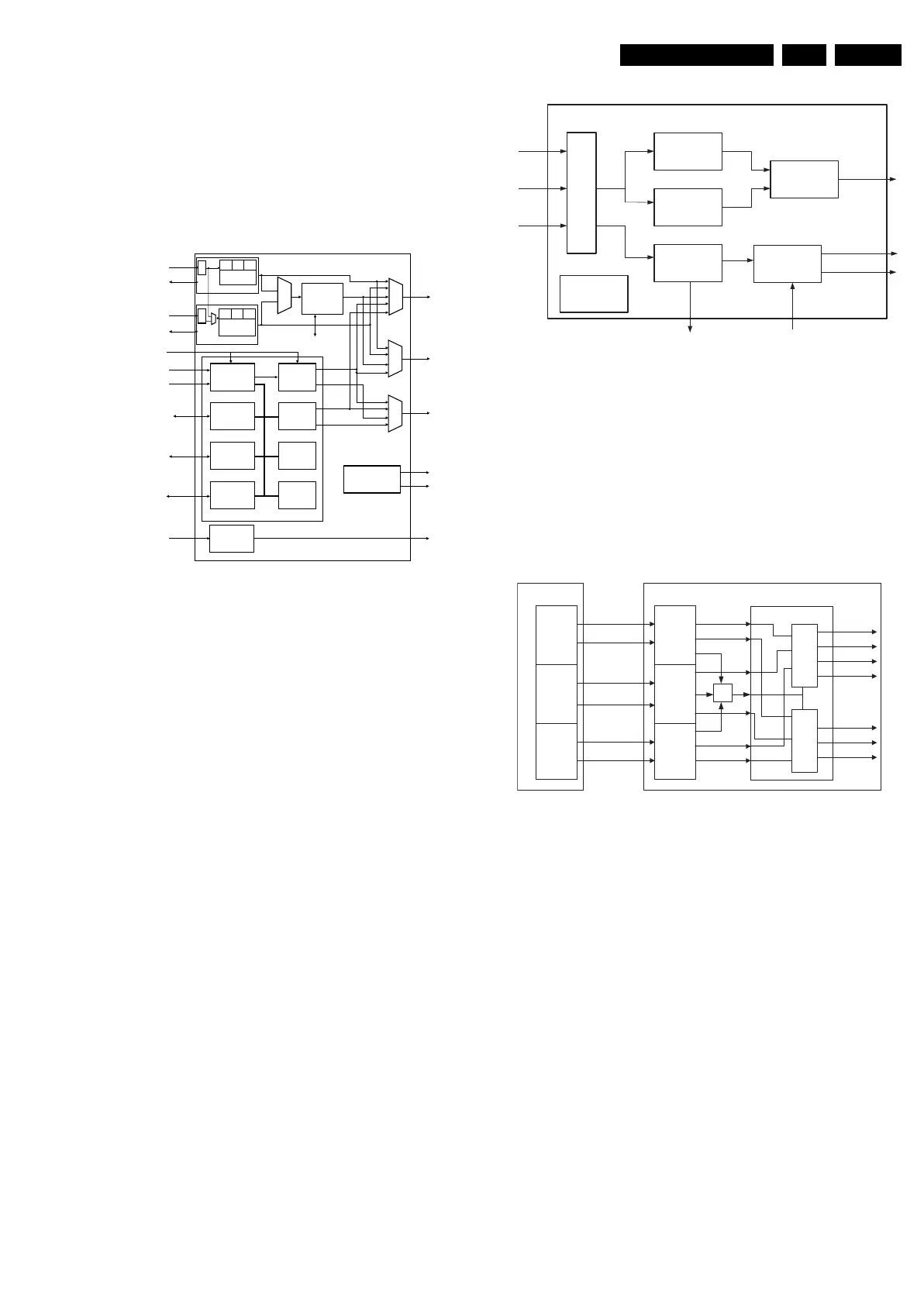
9.6 PNX2015
The functional blocks of the PNX2015 (item 7J00) are:
• Audio Video Input Processor (AVIP).
• 3D Comb Filter (COLUMBUS).
• High Definition MPEG Decoder (HD Subsystem).
• LVDS transmitter.
• Stand-by Processor for low-power control.
Figure 9-19 Block diagram PNX2015
These different blocks are described separately in the next
paragraphs.
9.7 PNX2015: AVIP
9.7.1 Introduction
The AVIP (Audio Video Input Processor) receives the digital
data via the I
2
D link (coming from MPIF). It reformats this data
and maps (synchronizes) the data to the clock of the AVIP.
Then a digital AGC is passed. After this, the video decoding is
performed in the VIDDEC-block of the AVIP. The decoded
video is sent to an output block, which formats the data to an
ITU-656 compatible standard data stream.
The AVIP power supply is 1.2 V and 3.3 V. To ensure
synchronization of video streams processed across the VIPER
and PNX2015 devices, a 27 MHz is coming from the VIPER.
The AVIP is I
2
C driven.
Initialization of this IC begins with a hard reset (MIPS-RESET)
provided by the VIPER. Besides video decoding, the AVIP is
also used for decoding and presentation of all audio output
streams in the system.
9.7.2 Block Diagrams
Below the main functions and features in the AVIP for video
and audio are given.
Figure 9-20 AVIP block diagram
Main AVIP function:
•I
2
D receiver.
• Colour decoding into ITU-601 compatible format (1fH/2fH).
• Interface with 3D comb filter (called Columbus in this
chassis).
• VBI data capture via DCU (Teletext, CC, etc.).
• ITU-656 formatting.
• Audio demodulation and decoding via DEMDEC.
• Audio processing and D/A conversion.
I
2
D Receiver
Figure 9-21 I
2
D receiver block diagram
The receiver block gets the serial data stream and converts it
to a parallel stream. This parallel data is fed to the "de-
multiplexer and formatter " block where the selected audio/
video stream is forwarded to the video and audio decoder for
further processing. This communication bus is completely
digital and very difficult to monitor.
The I
2
D link has the following characteristics.
• The data-link runs at 297 MHz / 594 Mbps.
• The driver rise/fall time is around 200 ps.
• The data-link uses differential signals.
AVIP-1
DLINK1
SYNC
COLUMBUS
0-9
10-19
VO-1
memory
controller
DV1
DV2
DV1MUX
DV3MUX
DV2MUX
PNX8550
direct
0-9
10-19
VO-2
HUB
PNX3000-1
AVIP-2
VIP
DLINK2
SYNC
PNX3000-2
DV4
DV5
video
SOUTH
TUNNEL
RX/TX
MBS
MEMORY
CONTROLLER
VMPG
LCD panel
PNX8550
DV3
PNX8550
NORTH
TUNNEL
RX/TX
LVDS_TX
TA, TB, TC, TD, TE, CLK
HD SUBSYSTEM
COLMUX
PNX2015
RGB,
HV
PNX8550
video
coprocessor
PNX8550
16-bit
200 MHz
DDR
D
L
I
N
K
D
L
I
N
K
VIDDEC
DCU
ITU
656
AUDIO
VIDDEC
DCU
ITU
656
AUDIO
TV
Microcontroller
PNX8550
Power Control
DSP/DEMDEC
DSP/DEMDEC
SYNC
F_15400_105.eps
180505
BLOCK DIAGRAM
E_14700_069.eps
310505
I2D
VIDDEC
DCU
DemDec
ITU-656
I2D1
I2D2
I2D3
CVBS/YC/YUV
SIF or L/R
I2Sout
I2SIn
ITU-656
Cvbs_yyc
VBI bytes
L
R
GP
Audio
Processing
E_14700_070.eps
300505
I2D
transmitter
I2D
receiver
L1/R1
YUV/ UV
yuv
SIF
CVBS
sec
L2/R2
CVBS
pri
/YC/
Y
yuv
I2D
transmitter
I2D
transmitter
I2D
receiver
I2D
receiver
I2D transmitter I2D AVIP
L2/R2
L1/R1
SIF
CVBS
pri
/Y
yc
Y
yuv
/ C
yc
UV
yuv
CVBS
sec
/ rexelpitlumed oediv
rettamrof
/ rexelpitlumed oidua
rettamrof
VAL1
VAL3
VAL2
VAL