Circuit Descriptions, Abbreviation List, and IC Data Sheets
EN 229JL2.1E AA 9.
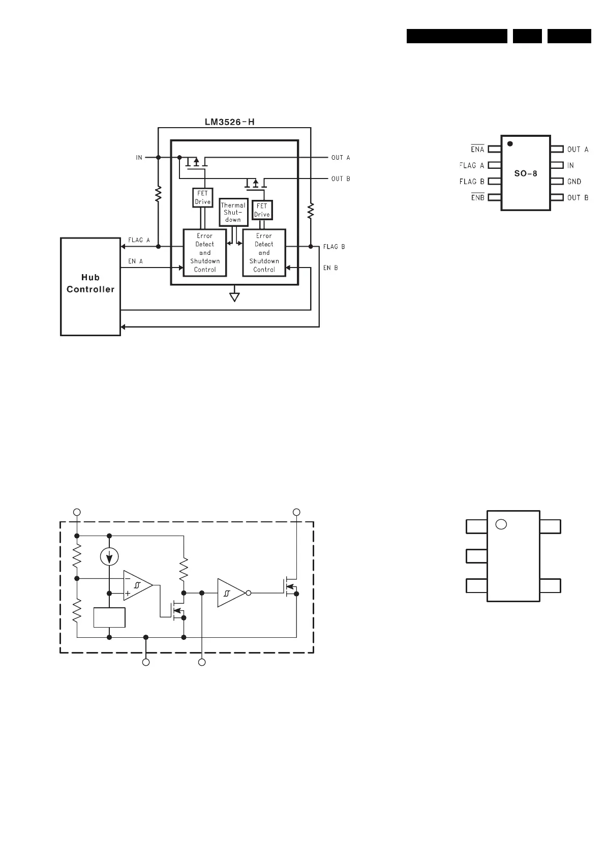
9.17.7 Diagram B7A, LM3526MX (IC 7Q01)
Figure 9-43 Internal block diagram and pin configuration
9.17.8 Diagram B8A, NCP303LSN (IC 7LB0 - 7LB4)
Figure 9-44 Internal block diagram and pin configuration
Block Diagram
Pin Configuration
F_15400_134.eps
230905
LM3526-L
Block Diagram
Pin Configuration
F_15400_133.eps
230905
NCP303LSNxxT1
Open Drain Output Configuration
V
ref
2 Input
3 Gnd
5C
D
R
D
1 Reset Output
1
3
N.C.
Reset
Output
2
Input
Ground
4
C
D
5
xxxYW
(Top View)
xxx = 302 or 303
Y = Year
W = Work Week
 Loading...