Circuit Descriptions, Abbreviation List, and IC Data Sheets
EN 230 JL2.1E AA9.
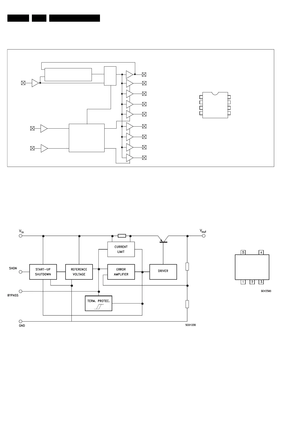
9.17.9 Diagram B8B, CY2305SC-1 (IC 7J08)
Figure 9-45 Internal block diagram and pin configuration
9.17.10 Diagram B9A, LD2985BM (IC 7G00)
Figure 9-46 Internal block diagram and pin configuration
Block Diagram
Pin Configuration
1
2
3
4
5
8
7
6
REF
CLK2
CLK1
GND
V
DD
CLKOUT
CLK4
CLK3
SOIC
Top View
PLL
MUX
Select Input
REF
S2
S1
CLKA1
CLKA2
CLKA3
CLKA4
CLKB1
CLKB2
CLKB3
CLKB4
Decoding
CLKOUT
E_14620_146.eps
200804
Block Diagram
LD2985BM
Pin Configuration
F_15710_165.eps
230905
SOT23-5L
 Loading...