Circuit Descriptions
EN 54 Q552.2E LA7.
2011-Jun-01
back to
div. table
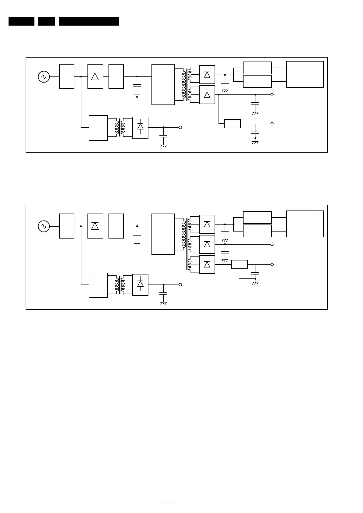
7.2.4 Functional block diagram LGIT Supply Units PLDE-P007A B & PLDK-P011AB
Figure 7-4 Functional block diagram LGIT supply units PLDE-P007A B & PLDK-P011AB
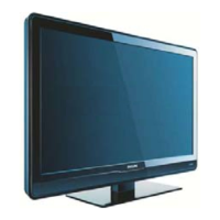
7.2.5 Functional block diagram LGIT Supply Unit PLDG-P009A(1.1)
Figure 7-5 Functional block diagram LGIT supply unit PLDG-P009A(1.1)
7.3 DC/DC Converters
The on-board DC/DC converters deliver the following voltages
(depending on set execution):
• +3V3-STANDBY, permanent voltage for the Stand-by
controller, LED/IR receiver and controls; connector 1M95
pin 1
• +12V, input from the power supply for TV550 common
(active mode); connector 1M95 pins 6, 7 and 8
• +24V, input from the power supply for DVB-S2 (in active
mode); connector 1M09 pins 1 and 2
• +1V1, core voltage supply for PNX855xx; has to be started
up first and switched "off" last (diagram B03B)
• +1V2, supply voltage for analogue blocks inside PNX855xx
• +1V8, supply voltage for DDR2 (diagram B03B)
• +2V5, supply voltage for analogue blocks inside PNX855xx
(see diagram B03E)
• +3V3, general supply voltage (diagram B03E)
• +5V, supply voltage for USB and CAM (diagram B03E)
• +5V-TUN, supply voltage for tuner (diagram B03E)
• +V-LNB, input voltage for LNB supply IC (item no. 7T50)
• +5V-DVBS, input intermediate supply voltage for DVB-S2
(diagram B08A)
• +3V3-DVBS, clean voltage for silicon tuner and DVB-S2
channel decoder
• +2V5-DVBS, clean voltage for DVB-S2 channel decoder
• +1V-DVBS, core voltage for DVB-S2 channel decoder.
A +12 V under-voltage detector (see diagram B03C) enables
the 12V to 3.3V and 12V to 5V DC/DC converters via the
ENABLE-3V3-5V line, and the 12V to 1.8V DC/DC converter
via the ENABLE-1V8 line. DETECT2 is the signal going to the
Stand-by microcontroller and ENABLE-3V3n is the signal
coming from the Stand-by microcontroller.
Diagram B03D contains the following linear stabilisers:
• +2V5 stabiliser, built around item no. 7UCO
• +5V-TUN stabiliser, built around items no. 7UA6 and 7UA7
• +1V2 stabiliser, built around items no. 7UA3 and 7UA4.
Diagram B08A contains the DVB-S2-related DC/DC
converters and -stabilisers:
• a +24V under-voltage detection circuitry is built around
item no. 7T04
• the switching frequency of the 24 to 14...20V switched
mode converter is 350 kHz (item no. 7T03 and +V-LNB
lines)
19103_003_110531.eps
110531
V(3.3 V)
STB
Boost
V
SSB
LED Driver 1
LED Driver 2
LED Backlight
V
(12.3 V)
(24.5 V)
SND
STBY
ACin
198 V-264V
90 V - 276 V
Line
filter
Resonant
converter
PFC
Diode
bridge
19103_004_110531.eps
110531
V(3.3 V)
STB
Reg
V
SSB
LED Driver 1
LED Driver 2
LED Backlight
V
(12.3 V)
(24.5 V)
SND
STBY
ACin
198 V-264V
90 V - 276 V
Line
filter
Resonant
converter
PFC
Diode
bridge