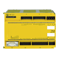
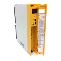
Commissioning
Operating Manual PNOZ m1p (ETH)
20878-EN-16
22
6.4 Commissioning the PNOZmulti control system for the first
time
Procedure:
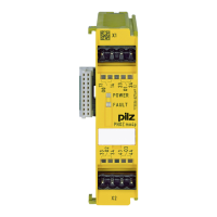
} Wire the inputs and outputs on the base unit and expansion modules in accordance
with the circuit diagram.
} Cascading output as auxiliary output: Connect the load to CO+ and A2, see connection
example.
} Connect the supply voltage:
– Supply voltage for the units (connector X7):
– Terminal A1: + 24VDC
– Terminal A2: 0 V
– Supply voltage for the semiconductor outputs (connector X2):
– 24 V terminal: + 24VDC
– 0V terminal: 0 V
Please note: Supply voltage must always be applied to X2 and X7, even if you are not us-
ing the semiconductor outputs.
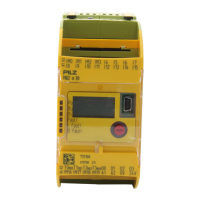
6.4.1 Load project from chip card
NOTICE
Chip contacting is only guaranteed if the contact surface is clean and un-
damaged. The chip's contact surface should therefore be protected from
contamination, contact and mechanical impact such as scratches.
Procedure:
} Insert the chip card containing the current project into the card slot on the base unit.
} Switch on the supply voltage.
6.4.2 Load project via integrated interface
Procedure:
} Insert a chip card into the chip card slot on the base unit.
} Connect the computer containing the PNOZmulti Configurator to the base unit via the
interface.
} Switch on the supply voltage.
} Download the project (see PNOZmulti Configurator's online help).
INFORMATION
You will need a PC with an Ethernet card in order to establish an Ethernet
connection.

 Loading...