142
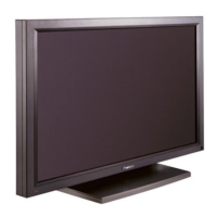
PDP-433CMX
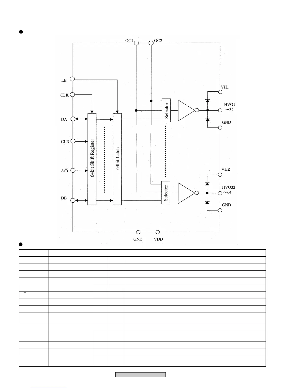
Pin Function
Block Diagram
Name Pin No. I/O Num. Function
CLK 86 I 1 Shift clock (start edge partial response)
DA 91 I/O 1 The serial data input of shifting register
DB 85 I/O 1 The serial data output of shifting register
LE 40 I 1 It output data done a latch of by "H" level
A/B 84 I 1 A shift directional control signal of shift register
CLR 92 I 1 It do data of shift register with "H" by "L" level
OC1 89 I 1 An output control terminal of HVO
OC2 90 I 1 An output control terminal of HVO
HVO
99, 100, 1-28
36-40, 48-76
O 64 High voltage drive output (HVO1 - HVO64)
VDD 88 − 1 Logic power supply
GND
30-32, 44-46
81-82, 93, 94-95
− 11 Standard potential. This is common to HVO1 - HVO64.
VH1 34, 35, 97, 98 − 4 The high potential circuit power supply which is common to HVO1 - HVO32
VH2 41, 42, 78, 79 − 4 The high potential circuit power supply which is common to HVO33 - HVO64
NC
29, 33, 43, 47
77, 80, 83, 96
− 8 It is the insulation electrically
 Loading...